This set of VLSI Multiple Choice Questions & Answers (MCQs) focuses on “Design for Testability”.
1. Design for testability is considered in production for chips because:
a) Manufactured chips are faulty and are required to be tested
b) The design of chips are required to be tested
c) Many chips are required to be tested within short interval of time which yields timely delivery for the customers
d) All of the mentioned
View Answer
Explanation: Design for testability is considered in production for chips because many chips are required to be tested within short interval of time which yields timely delivery for the customers.
2. The functions performed during chip testing are:
a) Detect faults in fabrication
b) Detect faults in design
c) Failures in functionality
d) All of the mentioned
View Answer
Explanation: The functions performed during chip testing are detecting faults in fabrication and design failures in functionality.
3. ATPG stands for:
a) Attenuated Transverse wave Pattern Generation
b) Automatic Test Pattern Generator
c) Aligned Test Parity Generator
d) None of the mentioned
View Answer
Explanation: ATPG is an Automatic Test Pattern Generator.
4. Delay fault is considered as:
a) Electrical fault
b) Logical fault
c) Physical defect
d) None of the Mentioned
View Answer
Explanation: Delay fault is considered a logical fault.
5. A metallic blob present between drain and the ground of the n-MOSFET inverter acts as:
a) Physical defect
b) Logical fault as output is stuck on 0
c) Electrical fault as resistor short
d) All of the mentioned
View Answer
Explanation: A metallic blob present between drain and the ground of the n-MOSFET inverter acts as Physical defect, Logical fault as output is stuck on 0, Electrical fault as resistor short.
6. High resistance short present between drain and ground of n-MOSFET inverter acts as:
a) Pull up delay error
b) Logical fault as output is stuck at 1
c) Electrical fault as transistor stuck on
d) All of the mentioned
View Answer
Explanation: High resistance short present between drain and ground of n-MOSFET inverter acts as Pull up delay error.
7. The defect present in the following MOSFET is:
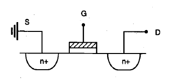
a) Logical stuck at 1
b) Logical stuck at 0
c) Physical defect
d) Electrical Transistor stuck open
View Answer
Explanation: The dimensions of the gate is less than the distance between source and drain.
8. The fault simulation detects faults by:
a) Test generation
b) Construction of fault Dictionaries
c) Design analysis under faults
d) All of the mentioned
View Answer
Explanation: None.
9. The ease with which the controller establishes specific signal value at each node by setting input values is known as:
a) Testability
b) Observability
c) Controllability
d) Manufacturability
View Answer
Explanation: Controllability is defined as the ease with which the controller establishes specific signal value at each node by setting input values.
10. The ease with which the controller determines signal value at any node by setting input values is known as:
a) Testability
b) Observability
c) Controllability
d) Manufacturability
View Answer
Explanation: Observability is defined as the ease with which the controller determines signal value at any node by setting input values.
11. The poor controllability circuits are:
a) Decoders
b) Clock generators
c) Circuits with feedback
d) All of the mentioned
View Answer
Explanation: None.
12. The circuits with poor observability are:
a) ROM
b) PLA
c) Sequential circuits with long feedback loops
d) All of the mentioned
View Answer
Explanation: None.
13. Large number of input vectors are used to set a particular node (1) or (0), to propagate an error at the node to output makes the circuit low on:
a) Testability
b) Observability
c) Controllability
d) All of the mentioned
View Answer
Explanation: The circuit is said to be low on Testability if large number of input vectors are used to set a particular node (1) or (0), to propagate an error at the node to output.
14. Divide and Conquer approach to large and complex circuits for testing is found in:
a) Partition and Mux Technique
b) Simplified automatic test pattern generation technique
c) Scan based technique
d) All of the mentioned
View Answer
Explanation: Divide and Conquer approach to large and complex circuits for testing is found in the partition and Mux technique.
15. LSSD stands for:
a) Linear system synchronous detection
b) Level sensitive system detection
c) Level sensitive scan design
d) Level sensitive scan detection
View Answer
Explanation: None.
Sanfoundry Global Education & Learning Series – VLSI.
To practice all areas of VLSI, here is complete set of 1000+ Multiple Choice Questions and Answers.
If you find a mistake in question / option / answer, kindly take a screenshot and email to [email protected]
