This set of Electronic Devices and Circuits Multiple Choice Questions & Answers (MCQs) focuses on “Transistor Switching Times”.
1. The collector current will not reach the steady state value instantaneously because of_________
a) stray capacitances
b) resistances
c) input blocking capacitances
d) coupling capacitance
View Answer
Explanation: When a pulse is given, the collector current will not reach the steady state value instantaneously because of stray capacitances. The charging and discharging of capacitance makes the current to reach a steady state value after a given time constant.
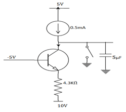
2. For the BJT, β=∞, VBEon=0.7V VCEsat=0.7V. The switch is initially closed. At t=0, it is opened. At which time the BJT leaves the active region?
a) 20ms
b) 50ms
c) 60ms
d) 70ms
View Answer
Explanation: At t < 0, the BJT is OFF in cut off region. IB=0 as β=∞, so IC=IE. When t > 0, switch opens and BJT is ON. The voltage across capacitor increases. From the input loop, -5-VBE-I(4.3K)+10=0 and gives I=1mA. IC1=1-0.5=0.5mA. VC1=0.7+4.3+10=-5V. IC1=C1dVC1/dt. From this equation, we get t=50ms.
3. The technique used to quickly switch off a transistor is by_________
a) reverse biasing its emitter to collector junction
b) reverse biasing its base to collector junction
c) reverse biasing its base to emitter junction
d) reverse biasing any junction
View Answer
Explanation: The technique used to quickly switch off a transistor is by reverse biasing its base to collector junction. It is demonstrated in a high voltage switching circuit. The advantage of this circuit is that it is not necessary to have high voltage control signal.
4. The disadvantage of using the method of reverse biasing base emitter junction is_________
a) high voltage control signal
b) low voltage control signal
c) output swing
d) incomplete switching of output
View Answer
Explanation: This method is used to quickly switch off a transistor is by reverse biasing its base to collector junction. It is demonstrated in a high voltage switching circuit. The disadvantage of using the method of reverse biasing base emitter junction is that the output does not switch completely to GND due to forward voltage drop of the diode.
5. Which of the following circuits helps in the applications of switching times?
a)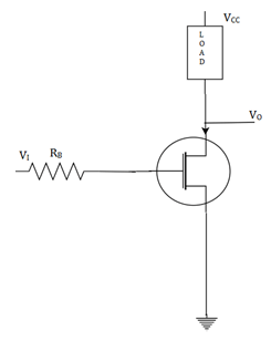
b)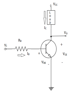
c)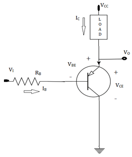
d)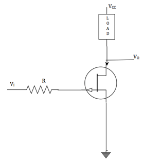
View Answer
Explanation: This is an inverter, in which the transistor in the circuit is switched between cut off and saturation. The load, for example, can be a motor or a light emitting diode or any other electrical device.
6. Which of the following helps in reducing the switching time of a transistor?
a) a resistor connected from base to ground
b) a resistor connected from emitter to ground
c) a capacitor connected from base to ground
d) a capacitor connected from emitter to ground
View Answer
Explanation: Connecting a resistor connected from base of a transistor to ground/negative voltage helps in reducing the switching the switching time of the transistor. When transistor saturate, there is stored charge in the base that must be removed before it turns off.
7. The time taken for a transistor to turn from saturation to cut off is _________
a) inversely proportional to charge carriers
b) directly proportional to charge carriers
c) charging time of the capacitor
d) discharging time of the capacitor
View Answer
Explanation: When sufficient charge carriers exist, the transistor goes into saturation. When the switch is turned off, in order to go into cut off, the charge carriers in the base region need to leave. The longer it takes to leave, the longer it takes for a transistor to turn from saturation to cut off.
8. The switching of power with a PNP transistor is called _________
a) sourcing current
b) sinking current
c) forward sourcing
d) reverse sinking
View Answer
Explanation: Sometimes DC current gain of a bipolar transistor is too low to directly switch the load current or voltage, so multiple switching transistors is used. The load is connected to ground and the transistor switches the power to it.
9. The base emitter voltage in a cut off region is _________
a) greater than 0.7V
b) equal to 0.7V
c) less than 0.7V
d) cannot be predicted
View Answer
Explanation: From the cut off characteristics, the base emitter voltage (VBE) in a cut off region is less than 0.7V. The cut off region can be considered as ‘off mode’. Here, VBE < 0.7 and IC=0. For a PNP transistor, the emitter potential must be negative with respect to the base.
10. Switching speed of P+ junction depends on _________
a) Mobility of minority carriers in P junction
b) Life time of minority carriers in P junction
c) Mobility of majority carriers in N junction
d) Life time of minority carriers in N junction
View Answer
Explanation: Switching leads to move holes in P region to N region as minority carriers. Removal of this accumulation determines switching speed. P+ regards to a diode in which the p type is doped excessively.
Sanfoundry Global Education & Learning Series – Electronic Devices and Circuits.
To practice all areas of Electronic Devices and Circuits, here is complete set of 1000+ Multiple Choice Questions and Answers.
If you find a mistake in question / option / answer, kindly take a screenshot and email to [email protected]
