This set of Electronic Devices and Circuits Multiple Choice Questions & Answers (MCQs) focuses on “Donor and Acceptor impurities”.
1. At what temperature the donor states are completely ionized?
a) 0 K
b) ROOM
c) 300K
d) 900K
View Answer
Explanation: At room temperature, the donors have donated their electrons to the conduction band.
2. The opposite of ionization takes place at which temperature?
a) 0 K
b) ROOM
c) 300 K
d) 900K
View Answer
Explanation: AT 0 K, all the donors and acceptors are in their lowest energy levels.
3. What do you mean by the tem ‘FREEZE-OUT’?
a) All the electrons are frozen at room temperature
b) None of the electrons are thermally elevated to the conduction band
c) All the electrons are in the conduction band
d) All the holes are in the valence band
View Answer
Explanation: Freeze out means none of the electrons are transmitted to the conduction band.
4. Which of the following expressions represent the correct formula for the density of electrons occupying the donor level?
a) nd=Nd-Nd+
b) nd=Nd-Nd–
c) nd=Nd+Nd+
d) nd=Nd+Nd–
View Answer
Explanation: The density of the electrons is equal to the electrons present in the substrate minus the number of donors present.
5. Which of the following band is just above the intrinsic Fermi level for n-type semiconductor?
a) Donor band
b) Valence band
c) Acceptor band
d) Conduction band
View Answer
Explanation: For n-type semiconductors, the donor band is just above the intrinsic Fermi level.
6. At absolute zero temperature, which level is above the Fermi energy level in the case of donors?
a) Donor energy level
b) Acceptor energy level
c) Conduction Band
d) Valence Band
View Answer
Explanation: At T=0 K, the tem exp(-∞)=0 in the expression of
Thus, EF>ED
So, only conduction band lies above the Fermi energy level.
7. At T=0 K, the location of Fermi level with respect to the Ec and Ed for the n type material is?
a) Above than conduction band
b) Midway
c) Lower than Ed
d) Greater than Ed
View Answer
Explanation: At T=0 K, the Fermi level of n band lies between the midway of Ec and Ed as intrinsic Fermi level always lies between the Ec and Ev.
8. At absolute zero temperature, which level is below the Fermi energy level in the case of acceptors?
a) Donor energy level
b) Valence Band
c) Conduction band
d) Acceptor energy level
View Answer
Explanation: At T=0 K, the tem exp(-∞)=0 in the expression of
So, only valence band lies below the Fermi energy level of the acceptors.
9. For the below n-type semiconductor, what is B knows as?
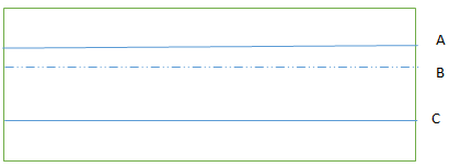
a) Valence Band
b) Conduction Band
c) Donor Energy level
d) Acceptor energy level
View Answer
Explanation: For n-type semiconductors, the donor energy level is always greater than the Fermi level energy.
10. For the below given figure, identify the correct option for satisfying the above semiconductor figure?
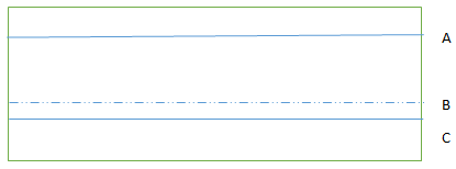
a) P type, A-Conduction band, B-donor energy band, C- Valence band
b) P type, A-Conduction band, B-acceptor energy band, C- Valence band
c) n type, A-Conduction band, B-donor energy band, C- Valence band
d) n type, A-Conduction band, B-acceptor energy band, C- Valence band
View Answer
Explanation: The given figure has B band below the intrinsic Fermi level, so that would be acceptor energy band and will be a p-type semiconductor.
Sanfoundry Global Education & Learning Series – Electronic Devices and Circuits.
To practice all areas of Electronic Devices and Circuits, here is complete set of 1000+ Multiple Choice Questions and Answers.
If you find a mistake in question / option / answer, kindly take a screenshot and email to [email protected]
