This set of Electronic Devices and Circuits Multiple Choice Questions & Answers (MCQs) focuses on “The CE Characteristics”.
1. The input characteristics of a CE transistor is_________
a) 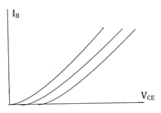
b) 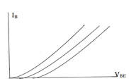
c) 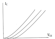
d) 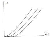
View Answer
Explanation: A graph of IB against VBE is drawn. The curve so obtained is known as input characteristics. The collector emitter voltage (VCE) is kept constant.
2. The input resistance is given by _________
a) ∆VCE/∆IB
b) ∆VBE/∆IB
c) ∆VBE/∆IC
d) ∆VBE/∆IE
View Answer
Explanation: The ratio of change in base emitter voltage (∆VBE) to resulting change in base current (∆IB) at constant collector emitter voltage (VCE) is defined as input resistance. This is denoted by ri.
3. Which of the following depicts the output characteristics of a CE transistor?
a) 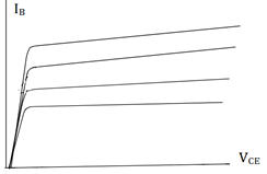
b) 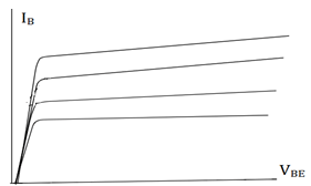
c) 
d) 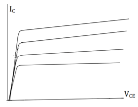
View Answer
Explanation: A graph of IC against VCE is drawn. The curve so obtained is known as output characteristics. The base current (IB) is kept constant.
4. The output resistance is given by _________
a) ∆VCE/∆IB
b) ∆VBE/∆IB
c) ∆VBE/∆IC
d) ∆VCE/∆IC
View Answer
Explanation: The ratio of change in collector emitter voltage (∆VCE) to resulting change in collector current (∆IC) at constant base current (IB) is defined as output resistance. This is denoted by ro.
5. Which of the following cases damage the transistor?
a) when VCE is increased too far
b) when VCE is decreased too far
c) when VBE is increased too far
d) when VBE is decreased too far
View Answer
Explanation: When VCE is increased too far, collector base junction completely breaks down and due to this avalanche breakdown, collector current increases rapidly. This is not shown in the characteristic. In this case, the transistor is damaged.
6. When the collector junction is reverse biased and emitter junction is forward biased, the operating region of the transistor is called_________
a) inverted region
b) active region
c) cut off region
d) cut in region
View Answer
Explanation: In the active region, for small values of base current, the effect of collector voltage over collector current is small while for large base currents this effect increases. The shape of characteristic here is same as that of CB transistors.
7. The small amount of current which flows even when base current IB=0 is called_________
a) IBEO
b) ICBO
c) ICEO
d) IC
View Answer
Explanation: In the cut off region, a small amount of collector current flows even when base current IB is zero. This is called ICEO. Since the main current is also zero, the transistor is said to be cut off.
8. A change in 700mV in base emitter voltage causes a change of 200µA in the base current. Determine the dynamic input resistance.
a) 2kΩ
b) 10kΩ
c) 3kΩ
d) 3.5kΩ
View Answer
Explanation: ro=∆VBE/∆IB
=700m/200µ=3.5kΩ.
9. The change in collector emitter voltage from 6V to 9V causes increase in collector current from 6mA to 6.3mA. Determine the dynamic output resistance.
a) 20kΩ
b) 10kΩ
c) 50kΩ
d) 60kΩ
View Answer
Explanation: ro=∆VCE/∆IC
=3/0.3m=10kΩ.
10. Which of the following points locates the quiescent point?
a) (IC, VCB)
b) (IE, VCE)
c) (IE, VCB)
d) (IC, VCE)
View Answer
Explanation: The quiescent point is best located between the cut off and saturation point. IE= VEE/RE, VCB=VCC-ICRL. It is denoted by ‘Q’.
Sanfoundry Global Education & Learning Series – Electronic Devices and Circuits.
To practice all areas of Electronic Devices and Circuits, here is complete set of 1000+ Multiple Choice Questions and Answers.
If you find a mistake in question / option / answer, kindly take a screenshot and email to [email protected]
