This set of Electronic Devices and Circuits Multiple Choice Questions & Answers (MCQs) focuses on “MOSFET in Amplfier Design”.
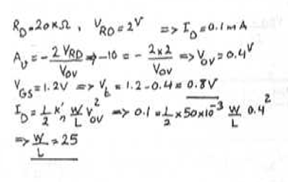
1. Various measurements are made on an NMOS amplifier for which the drain resistor RD is 20 kΩ. First, DC measurements show the voltage across the drain resistor, VRD, to be 2 V and the gate-to-source bias voltage to be 1.2 V. Then, ac measurements with small signals show the voltage gain to be −10 V/V. What is the value of Vt for this transistor?
a) 0.7V
b) 0.8V
c) 0.9V
d) 1.0V
View Answer
2. Various measurements are made on an NMOS amplifier for which the drain resistor RD is 20 kΩ. First, DC measurements show the voltage across the drain resistor, VRD, to be 2 V and the gate-to-source bias voltage to be 1.2 V. Then, ac measurements with small signals show the voltage gain to be −10 V/V. If the process transconductance parameter is 50μA/V2, what is the MOSFET’s W/L?
a) 25
b) 50
c) 75
d) 100
View Answer
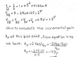
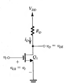
3. Consider the amplifier below for the case VDD = 5 V, RD = 24 kΩ, (W/L) = 1 mA/V2, and Vt = 1 V. If the amplifier is biased to operate with an overdrive voltage VOV of 0.5 V, find the incremental gain at the bias point.
a) -3 V/V
b) -6 V/V
c) -9 V/V
d) -12 V/V
View Answer
4. Consider the amplifier below for the case VDD = 5 V, RD = 24 kΩ, (W/L) = 1 mA/V2, and Vt = 1 V. For amplifier biased to operate with an overdrive voltage of 0.5V, and disregarding the distortion caused by the MOSFET’s square-law characteristic, what is the largest amplitude of a sine-wave voltage signal that can be applied at the input while the transistor remains in saturation?

a) 1.61 V
b) 1.5 V
c) 0.11 V
d) 3.11 V
View Answer
Explanation: Use the standard mathematical formula to obtain the result.
5. Consider the amplifier below for the case VDD = 5 V, RD = 24 kΩ, (W/L) = 1 mA/V2, and Vt = 1 V. For the input signal of 1.5V what is the value of the gain value obtained?

a) -12.24 V/V
b) -12.44 V/V
c) -12.64 V/V
d) -12.84 V/V
View Answer
Explanation: The amplitude of the output voltage signal that results is approximately equal to Voq – VOB = 2 – 0.61 = 1.39v.
The gain implied by amplitude is
Gain = -1.39/0.11 = -12.64 V/V.
6. Which of the following is the fastest switching device?
a) JEFT
b) Triode
c) MOSFET
d) BJT
View Answer
Explanation: MOSFET is the fastest switching device among the given four options.
7. Bias point is also referred by the name
a) DC Operating Point
b) Quiescent Point
c) None of the mentioned
d) All of the mentioned
View Answer
Explanation: Bias point is called dc operating point as the MOSFET functions best at this point. Also since at the bias point no signal component is present it is called quiescent point (he reason why it is represented by the symbol ‘Q’)
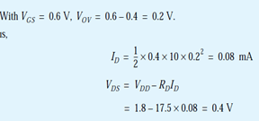
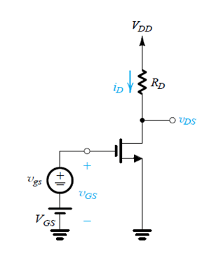
8. Consider the amplifier circuit shown below. The transistor is specified to have Vt = 0.4 V, kn = 0.4 mA/V2, W/L = 10 and λ = 0. Also, let VDD = 1.8V, RD = 17.5kΩ, VGS = 0.6V and vgs = 0V. Find ID.
a) 0.08 mA
b) 0.16 mA
c) 0.4 mA
d) 0.8 mA
View Answer
9. Consider the amplifier circuit shown below. The transistor is specified to have Vt = 0.4 V, kn = 0.4 mA/V2, W/L = 10 and λ = 0. Also, let VDD = 1.8V, RD = 17.5kΩ, VGS = 0.6V and vgs = 0V. Find VDS.

a) 0.1V
b) 0.2 V
c) 0.4 V
d) 0.8 V
View Answer
10. Consider the amplifier circuit shown below. The transistor is specified to have Vt = 0.4 V, kn = 0.4 mA/V2, W/L = 10 and λ = 0. Also, let VDD = 1.8V, RD = 17.5kΩ, VGS = 0.6V and vgs = 0V. Find Av.

a) -12 V/V
b) -14 V/V
c) -16 V/V
d) -18 V/V
View Answer
Explanation: Av = – kn Vov RD
= -0.4 * 10 * 0.2 * 17.5
= – 14.4v
Sanfoundry Global Education & Learning Series – Electronic Devices and Circuits.
To practice all areas of Electronic Devices and Circuits, here is complete set of 1000+ Multiple Choice Questions and Answers.
If you find a mistake in question / option / answer, kindly take a screenshot and email to [email protected]
