This set of Electronic Devices and Circuits Multiple Choice Questions & Answers (MCQs) focuses on “DC Load Lines”.
1. Which of the following depicts the DC load line?
a) 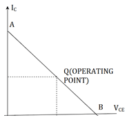
b) 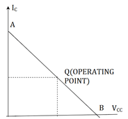
c) 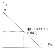
d) 
View Answer
Explanation: In transistor circuit analysis, sometimes it is required to know the collector currents for various collector emitter voltages. The one way is to draw its load line. We require the cut off and saturation points.
2. For the circuit shown, find the quiescent point.
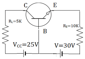
a) (10V, 4mA)
b) (4V, 10mA)
c) (10V, 3mA)
d) (3mA, 10V)
View Answer
Explanation: We know, IE=VEE/RE=30/10kΩ=3mA
IC=α IE =IE =3mA
VCB=VCC-ICRL=25-15=10V. So, quiescent point is (10V, 3mA).
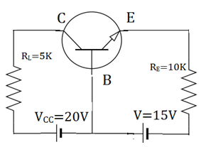
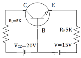
3. Which of the following depicts the load line for the circuit shown below?
a) 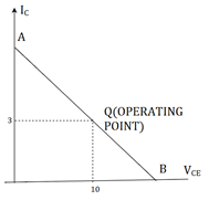
b) 
c)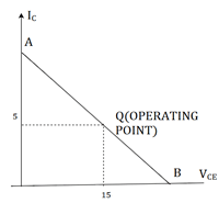
d)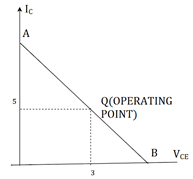
View Answer
Explanation: We know, IE=VEE/RE=15/5kΩ=3mA
IC=α IE =IE =3mA
VCB=VCC-ICRL=20-15=5V. So, quiescent point is (5V, 3mA).
4. For the circuit shown, find the quiescent point.
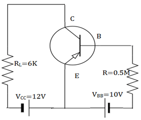
a) (6V, 1mA)
b) (4V, 10mA)
c) (10V, 3mA)
d) (3mA, 10V)
View Answer
Explanation: We know, VCE=12V
(IC)SAT =VCC/RL=12/6K=2mA. IB=10V/0.5M=20µA. IC= βIB=1mA. I
VCE=VCC-ICRL=12-1*6=6V. So, quiescent point is (6V, 1mA).
5. Which of the following depicts the load line for the given circuit?
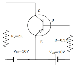
a) 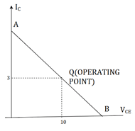
b) 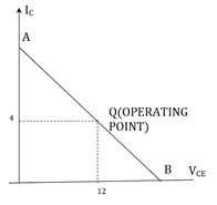
c) 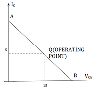
d) 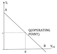
View Answer
Explanation: We know, VCE=6V
(IC)SAT =VCC/RL=10/2K=5mA. IB=10V/0.5M=20µA. IC= βIB=1mA. I
VCE=VCC-ICRL=10-1*2=8V. So, quiescent point is (8V, 1mA).
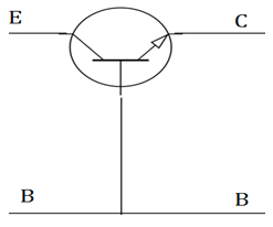
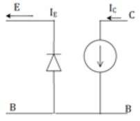
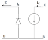
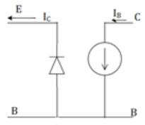
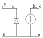
6. The DC equivalent circuit for an NPN common base circuit is.
a)
b)
c)
d)
View Answer
Explanation: In the common base circuit, the emitter diode acts like a forward biased ideal diode, while collector diode acts as a current source due to transistor action. Thus an ideal transistor may be regarded as a rectifier diode in the emitter and a current source at collector.
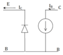
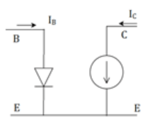
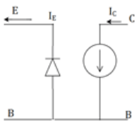
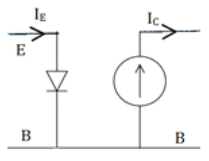
7. The DC equivalent circuit for an NPN common emitter circuit is.
a)
b)
c)
d)
View Answer
Explanation: In the common emitter circuit, the ideal transistor may be regarded as a rectifier diode in the base circuit and a current source in the collector circuit. In the current source, the direction of arrow points in direction of conventional current.
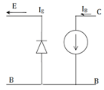
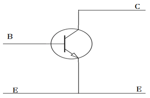
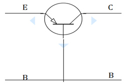
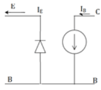
8. What is the other representation of the given PNP transistor connected in common emitter configuration?
a)
b)
c)
d)
View Answer
Explanation: The emitter junction is forward biased with the help of battery VEE by which, negative of the battery is connected to the emitter while positive is connected to base. RE is the emitter resistance. The collector junction is reversed biased.
9. What is the DC characteristic used to prove that the transistor is indeed biased in saturation mode?
a) IC = βIB
b) IC > βIB
c) IC >> βIB
d) IC < βIB
View Answer
Explanation: When in a transistor is driven into saturation, we use VCE(SAT) as another linear parameter. In, addition when a transistor is biased in saturation mode, we have IC < βIB. This characteristic used to prove that the transistor is indeed biased in saturation mode.
10. For the circuit shown, find the quiescent point.
a) (10V, 4mA)
b) (4V, 10mA)
c) (10V, 3mA)
d) (3mA, 10V)
View Answer
Explanation: We know, IE=VEE/RE=10/5kΩ=2mA
IC=α IE =IE =2mA
VCB=VCC-ICRL=20-10=10V. So, quiescent point is (10V, 2mA).
Sanfoundry Global Education & Learning Series – Electronic Devices and Circuits.
To practice all areas of Electronic Devices and Circuits, here is complete set of 1000+ Multiple Choice Questions and Answers.
If you find a mistake in question / option / answer, kindly take a screenshot and email to [email protected]
