This set of Electronic Devices and Circuits Multiple Choice Questions & Answers (MCQs) focuses on “Transistor as a Switch”.
1. In which region a transistor acts as an open switch?
a) cut off region
b) inverted region
c) active region
d) saturated region
View Answer
Explanation: In this mode, both the junctions are reverse biased. The transistor has practically zero current because the emitter does not emit charge carriers to the base. There is negligibility current due to minority carriers. In this mode the transistor acts as an open switch.
2. In which region a transistor acts as a closed switch?
a) cut off region
b) inverted region
c) active region
d) saturated region
View Answer
Explanation: In this mode, both the junctions are forward biased. The negative terminal of the battery is connected to the emitter. The collector current becomes independent of base current. In this mode the transistor acts as a closed switch.
3. Which of the following circuits act as a switch?
a)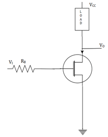
b)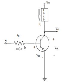
c)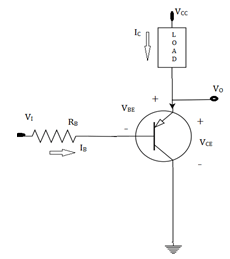
d)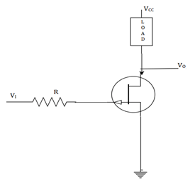
View Answer
Explanation: This is an inverter, in which the transistor in the circuit is switched between cut off and saturation. The load, for example, can be a motor or a light emitting diode or any other electrical device.
4. The current which is helpful for LED to turn on is_________
a) emitter current
b) base current
c) collector current
d) depends on bias
View Answer
Explanation: Depending on the type of load, a collector current is induced that would turn on the motor or LED. The transistor in the circuit is switched between cut off and saturation. The load, for example, can be a motor or a light emitting diode or any other electrical device.
5. Which of the following statements is true?
a) Solid state switches are applications for an AC output
b) LED’s can be driven by transistor logics
c) Only NPN transistor can be used as a switch
d) Transistor operates as a switch only in active region
View Answer
Explanation: Output devices like LED’s only require a few milliamps at logic level DC voltages and can therefore be driven directly by the output of a logic gate. However, high power devices such as motors or lamps require more power than that supplied by an ordinary logic gate so transistor switches are used.
6. The base emitter voltage in a cut off region is_________
a) greater than 0.7V
b) equal to 0.7V
c) less than 0.7V
d) cannot be predicted
View Answer
Explanation: From the cut off characteristics, the base emitter voltage (VBE) in a cut off region is less than 0.7V. The cut off region can be considered as ‘off mode’. Here, VBE > 0.7 and IC=0. For a PNP transistor, the emitter potential must be negative with respect to the base.
7. In saturation region, the depletion layer_________
a) increases linearly with carrier concentration
b) decreases linearly with carrier concentration
c) increases by increasing the emitter current
d) decreases by decreasing the emitter voltage drop
View Answer
Explanation: Here, the transistor will be biased so that maximum amount of base current is applied, resulting in maximum collector current resulting in minimum emitter voltage drop which results in depletion layer as small as possible and maximum current flows through the transistor.
8. The base emitter voltage in a saturation region is_________
a) greater than 0.7V
b) equal to 0.7V
c) less than 0.7V
d) cannot be predicted
View Answer
Explanation: From the saturation mode characteristics, the transistor acts as a single pole single throw solid state switch. A zero collector current flows. With a positive signal applied to the base of transistor it turns on like a closed switch.
9. The switching of power with a PNP transistor is called_________
a) sourcing current
b) sinking current
c) forward sourcing
d) reverse sinking
View Answer
Explanation: Sometimes DC current gain of a bipolar transistor is too low to directly switch the load current or voltage, so multiple switching transistors is used. The load is connected to ground and the transistor switches the power to it.
10. The switching of power with a NPN transistor is called_________
a) sourcing current
b) sinking current
c) forward sourcing
d) reverse sinking
View Answer
Explanation: Sometimes DC current gain of a bipolar transistor is too low to directly switch the load current or voltage, so multiple switching transistors is used. The load is connected to supply and the transistor switches the power to it.
Sanfoundry Global Education & Learning Series – Electronic Devices and Circuits.
To practice all areas of Electronic Devices and Circuits, here is complete set of 1000+ Multiple Choice Questions and Answers.
If you find a mistake in question / option / answer, kindly take a screenshot and email to [email protected]
