This set of Electronic Devices and Circuits Problems focuses on “Biasing in MOS Amplifier Circuit”.
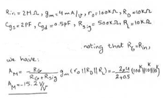
1. A discrete MOSFET common source amplifier has Rin = 2 MΩ, gmm = 4mA/V, ro = 100 kΩ, RD = 10 kΩ, Cgs = 2pF and Cgd = 0.5pF. The amplifier is fed from a voltage source with an internal resistance of 500 kΩ and Is connected to the a load of 10 kΩ. The value of the overall mixed gain AM is?
a) -15.2 V/V
b) -16.2 V/V
c) -17.2 V/V
d) -18.2 V/V
View Answer
Explanation:
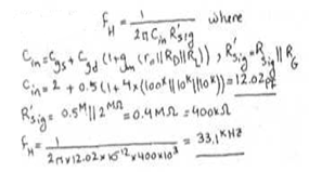
2. A discrete MOSFET common source amplifier has Rin = 2 MΩ, gmm = 4mA/V, ro = 100 kΩ, RD = 10 kΩ, Cgs = 2pF and Cgd = 0.5pF. The amplifier is fed from a voltage source with an internal resistance of 500 kΩ and Is connected to the a load of 10 kΩ. The upper 3-db frequency fH is?
a) 11.1 kHz
b) 22.1 kHz
c) 33.1 kHz
d) 44.1 kHz
View Answer
Explanation:
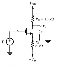
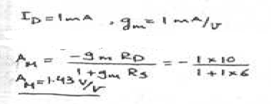
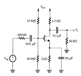
3. The amplifier in the figure shown below is biased to operate at ID = 1mA and gm = 1mA/V. Find the midband gain.
a) 0.43 V/V
b) 1.43 V/V
c) 2.43 V/V
d) 3.43 V/V
View Answer
Explanation:
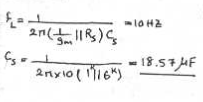
4. The amplifier in the figure shown below is biased to operate at ID = 1mA and gm = 1mA/V. Find the value of CS that places FL at 10Hz.
a) 6.57 µF
b) 12.57 µF
c) 18.57 µF
d) 24.57 µF
View Answer
Explanation:
5. In the NMOS transistor of the circuit shown below is biased to have gm = 1mA/V and r0 = 100 kΩ. Find AM.
a) 1.02 V/V
b) 2.04 V/V
c) 3.06 V/V
d) 4.08 V/V
View Answer
Explanation:
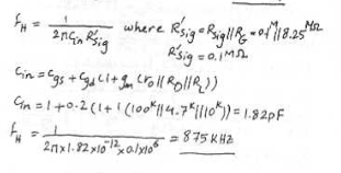
6. In the NMOS transistor of the circuit shown below is biased to have gm = 1mA/V and r0 = 100 kΩ. Find fH if Cgs = 1 pF and Cgd = 0.2 pF.
a) 875 kHz
b) 875 kHz
c) 875 kHz
d) 875 kHz
View Answer
Explanation:
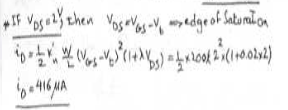
7. For a particular depletion mode NMOS device, Vt = -2V, kn W/L = 200 µA/V2 and λ = 0.02V-1. For VDS = 2V. What is the drain current that flows
a) 104 µA
b) 208 µA
c) 312µA
d) 416 µA
View Answer
Explanation:
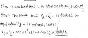
8. For a particular depletion mode NMOS device, Vt = -2V, kn W/L = 200 µA/V2 and λ = 0.02V-1. For VDS = 2V. What is the value of the drain current if both L and W are doubled?
a) 408 µA
b) 412 µA
c) 416 µA
d) 420 µA
View Answer
Explanation:
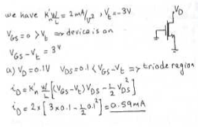
9. A depletion type N channel MOSFEt with knW/L = 2 mA/V2 and Vt = 3V has its source and gate grounded. For Vd = 0.1V and neglecting channel length modulating effect. Find drain current.
a) 1.18 mA
b) 0.89 mA
c) 0.59 mA
d) 0.3 mA
View Answer
Explanation:
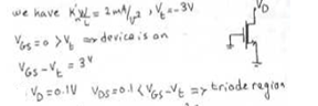
10. A depletion type N channel MOSFEt with knW/L = 2 mA/V2 and Vt = 3V has its source and gate grounded. For Vd = 0.1V and neglecting channel length modulating effect. In which region is the triode operating?
a) Triode region
b) End of saturation region
c) Saturation region
d) None of the mentioned
View Answer
Explanation:
Sanfoundry Global Education & Learning Series – Electronic Devices and Circuits.
To practice all areas of Electronic Devices and Circuits Problems, here is complete set of 1000+ Multiple Choice Questions and Answers.
If you find a mistake in question / option / answer, kindly take a screenshot and email to [email protected]
