This set of Tough Electronic Devices and Circuits Questions and Answers focuses on “MOSFETs Circuits at DC”.
1. The transistor in the circuit shown below has kn = 0.4 mA/V2, Vt = 0.5 V and λ = 0. Operation at the edge of saturation is obtained when
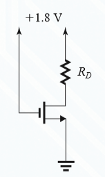
a) (W/L)RD = 0.5 kΩ
b) (W/L)RD = 1.0 kΩ
c) (W/L)RD = 1.5 kΩ
d) (W/L)RD = 2.0 kΩ
View Answer
Explanation: Use the standard formula for edge saturation.
2. The PMOS transistor in the circuit shown has Vt = −0.7 V, μpCox = 60 μA/V2, L = 0.8 μm, and λ = 0. Find the value of R in order to establish a drain current of 0.115 mA and a voltage VD of 3.5 V.
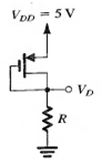
a) 12.5 KΩ
b) 25 kΩ
c) 37.5 kΩ
d) 50 kΩ
View Answer
Explanation:
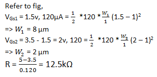
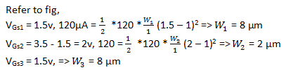
3. The NMOS transistors in the circuit shown have Vt = 1 V, μnCOX = 120 μA/V2, λ = 0, and L1 = L2 = L3 = 1μm. Then which of the following is not the value of the width of these MOSFETs shown
a) 2 µm
b) 8µm
c) All of the mentioned
d) None of the mentioned
View Answer
Explanation:
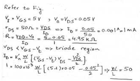
4. The MOSFET shown has Vt = 1V, kn = 100µA/V2 and λ = 0. Find the required values of W/L and of R so that when vI = VDD = +5 V, rDS = 50 Ω, and VO = 50 mV.
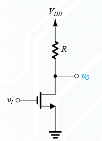
a) W/L = 25 and R = 4.95 kΩ
b) W/L = 25 and R = 9.90 kΩ
c) W/L = 50 and R = 4.95 kΩ
d) W/L = 50 and R = 9.90 kΩ
View Answer
Explanation:
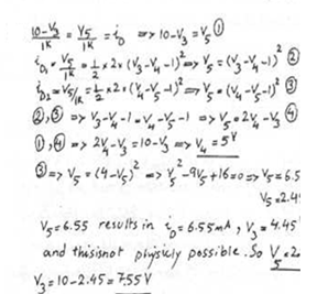
5. For each of the circuits shown find the labeled voltages. For all transistors, kn(W/L) = 1 mA/V2, Vt = 2V, and λ = 0. Find V3
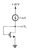
a) 2.41V
b) 3.41V
c) 4.41V
d) 1.41V
View Answer
Explanation: V3 = 10- 4 * 2 + 1.4 = 3.4v.
6. For each of the circuits shown find the labeled voltages. For all transistors, kn(W/L) = 1 mA/V2, Vt = 2V, and λ = 0. Find V4 and V5
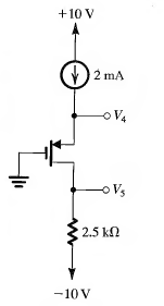
a) 4V and -5V respectively
b) -4V and 5V respectively
c) 4V and 5V respectively
d) -4V and -5V respectively
View Answer
Explanation:
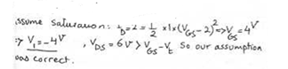
7. For each of the circuits shown find the labeled voltages. For all transistors, kn(W/L) = 1 mA/V2, Vt = 2V, and λ = 0. Find V1 and V2
a) 2V and -4V
b) -2V and 4V
c) 2V and 4V
d) -2V and -4V
View Answer
Explanation: ID = 1 = 1⁄2 * 1 * (VGS – 2)2 => VGS = 3.41v.
V3 = 3.41v.
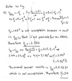
8. For each of the circuits shown find the labeled node voltages. The NMOS transistors have Vt = 1 V and kn( W/L ) = 2 mA/V2 and λ = 0. Find V1 and V2
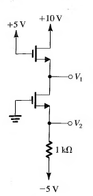
a) 2.44 and -1.28 V
b) 2.44 and -2.56 V
c) 1.22 and -2.56 V
d) 1.22 and -1.28 V
View Answer
Explanation:
9. For each of the circuits shown find the labeled node voltages. The NMOS transistors have Vt = 1 V and kn( W/L ) = 2 mA/V2 and λ = 0. Find V3 and V4
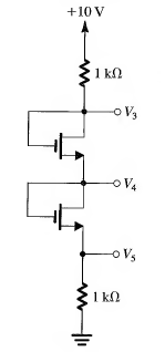
a) 3.775V and 5V
b) 3.775V and 2.55V
c) 7.55V and 2.55V
d) 7.555V and 5V
View Answer
Explanation:
10. For the PMOS transistor in the circuit shown kn= 8 µA/V2, W/L = 25,|Vtp| = 1V and I = 100μA. For what value of R is VSD = VSG?
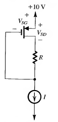
a) 0 Ω
b) 12.45 kΩ
c) 25.9 kΩ
d) 38.35 kΩ
View Answer
Explanation: VSG will be equal to VSD only when the resistance shown is zero or in other words there should not be any resistance.
Sanfoundry Global Education & Learning Series – Electronic Devices and Circuits.
To practice Tough questions and answers on all areas of Electronic Devices and Circuits, here is complete set of 1000+ Multiple Choice Questions and Answers.
If you find a mistake in question / option / answer, kindly take a screenshot and email to [email protected]
