This set of Electronic Devices and Circuits Multiple Choice Questions & Answers (MCQs) focuses on “PN Diode Switching Times”.
1. Diode acts as a short circuit when switched from forward to reverse bias for some time due to______
a) Accumulation of minority charge carriers when it’s in forward bias
b) Accumulation of majority charge carriers when it’s in forward bias
c) Accumulation of minority charge carriers when it’s in reverse bias
d) Accumulation of majority charge carrier when it’s in reverse bias
View Answer
Explanation: When a diode is switched suddenly, it persists the conducting property for a short time in its reverse bias also. This leads to excess minority charge carrier settlement at potential barrier. Hence acts as a short circuit.
2. Reverse recovery time for a diode is?
a) Time taken to eliminate excess minority charge carriers
b) Sum of storage time (TS) and transition time (TT)
c) Time taken to eliminate excess majority charge carriers
d) Time elapsed to return to non conduction state
View Answer
Explanation: The time period for which diode remains in conduction state even in reverse direction is called storage time. The time elapsed to return the non conduction state is called transition time. Their sum is called reverse recovery time.
3. Switching speed of P+ junction depends on.
a) Mobility of minority carriers in P junction
b) Life time of minority carriers in P junction
c) Mobility of majority carriers in N junction
d) Life time of minority carriers in N junction
View Answer
Explanation: Switching leads to move holes in P region to N region as minority carriers. Removal of this accumulation determines switching speed. P+ regards to a diode in which the p type is doped excessively.
4. Time taken for a diode to reach 90% of its final value when switched from steady state is______
a) 2.3*time constant
b) 2.2*time constant
c) 1.5*time constant
d) equals the time constant
View Answer
Explanation: Time constant = RC. To reach 90% of the final value, time taken is 2.2 of RC. Time constant is the time required to discharge the capacitor, through the resistor, by 36.8%.
5. Which of the following are true?
1) In reverse bias, the diode undergoes stages of storage and transition times
2) Minority charge carriers accumulation makes the diode as a short circuit
3) Storage time is the sum of recovery and transition times
a) 1 only
b) 2 and 3
c) 3 only
d) 1 and 2 only
View Answer
Explanation: When a diode is switched from forward to reverse bias, storage and transition times takes place. The accumulation time or the life time of minority carriers makes it a short circuit. The conduction property is holds for a short period of time in reverse bias also.
6. In a circuit below, the switch is at position 1 at t<0 and at position 2 when t=0. Assume diode has zero voltage drop and storage time. For 0<t<ts, the VR at 1k ohm resistor is given by_____
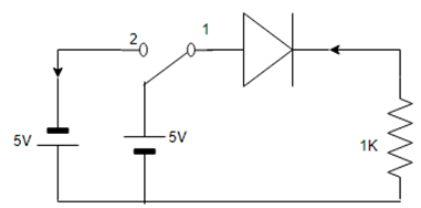
a) 5V
b) -5V
c) 0v
d) 10V
View Answer
Explanation: At position ‘1’ when connected to +5V, the diode is forward biased and acts as a short circuit. So, VR is 5V. For 0<t<ts VR is -5V as the diode is in reverse bias. But it holds the conductive property within the storage time period. So, V is -5V.
7. The switch is at position shown in the figure initially and steady state is from t=0 to t=to. The switch suddenly is thrown to the other position. The current flowing through the 10K resistor from t=0 is?
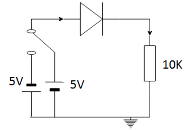
a) 1mA
b) 2mA
c) -2mA
d) -1mA
View Answer
Explanation: Initially, the diode is in forward bias. When suddenly switched to reverse bias, upto a storage time limit, it conducts during storage time period.
We know that, current I=V/R=-20/10K=-2mA.
8. A PN junction diode with 100Ω resistor is forward biased such that 100A current flows. If voltage across this combination is instantaneously reversed to 10V at t=0, the reverse current that flows through diode at t=0 is?
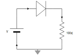
a) 10mA
b) 100mA
c) -100mA
d) -10mA
View Answer
Explanation: At t=0, V=-10V. During storage time, current still flows.
We know that,
current I=V/R=10/100Ω=100mA from N to P region.
9. The delay in switching between the ON and OFF states is due to _________
a) The time required to change amount of excess minority carriers stored in quasi-neutral regions
b) The time required to change amount of excess majority carriers stored in quasi-neutral regions
c) The conduction between storage time and recovery time
d) The exponential increase in carriers in N region
View Answer
Explanation: When switched instantaneously it stays in a quasi state i.e.., temporary state which stores charges. The delay is produced due to this charge settlement. The diode needs to discharge these excess carriers in order to return the non conduction stage.
10. The delay time can be reduced by?
a) decreasing lifetime and increasing ratio of reverse to forward current
b) increasing lifetime and decreasing ratio of reverse to forward current
c) increasing lifetime and increasing ratio of reverse to forward current
d) decreasing lifetime and decreasing ratio of reverse to forward current
View Answer
Explanation: When the current increases the depletion layer decreases and the storage and transition time decreases. A decreased depletion layer can easily discharge the excess carrier and thereby lessens the delay time.
Sanfoundry Global Education & Learning Series – Electronic Devices and Circuits.
To practice all areas of Electronic Devices and Circuits, here is complete set of 1000+ Multiple Choice Questions and Answers.
If you find a mistake in question / option / answer, kindly take a screenshot and email to [email protected]
