This set of Electronic Devices and Circuits Multiple Choice Questions & Answers (MCQs) focuses on “BJT in Amplifier Design”.
1. Find the maximum allowed output negative swing without the transistor entering saturation, and
a) 1.27 mV
b) 1.47 mV
c) 1.67 mV
d) 1.87 mV
View Answer
Explanation:
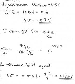
2. The corresponding maximum input signal permitted is
a) 1.64 mV
b) 1.74 mV
c) 1.84 mV
d) 1.94 mV
View Answer
Explanation: If we assume linear operation right to saturation we can use the gain Av to calculate the maximum input signal. Thus for an output swing ∆ Vo = 0.8 we have
∆ Vi = ∆ Vo / Av = -0.7 / -360 = 1.94 mV.
3. For the amplifier circuit in the below figure with Vcc = +10 V, Rc = 1 kΩ and the DC collector bias current equal to Ic. Find the voltage gain.
a) 100 Ic
b) 200 Ic
c) 400 Ic
d) 800 Ic
View Answer
Explanation:
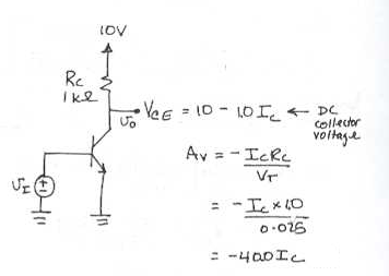
4. For the amplifier circuit in the below figure with Vcc = +10 V, Rc = 1 kΩ and the DC collector bias current equal to Ic. The maximum possible positive output signal swing as determined by the need to keep the transistor in the active region.
a) 9.7 + Ic
b) 9.7 – Ic
c) 10.3 + Ic
d) 10.3 – Ic
View Answer
Explanation: Assuming the output voltage Vo = 0.3v is the lowest Vce to stay out of saturation.
Vo = 0.3 = 10 – IcRc
= 10 – IcRc + ∆Vo
∆ Vo = -10 + 0.3 + Ic*1.
5. For the amplifier circuit in the below figure with Vcc = +10 V, Rc = 1 kΩ and the DC collector bias current equal to Ic. The maximum possible negative output signal swing as determined by the need to keep the transistor in the active region.
a) 0.1 Ic
b) Ic
c) 10 Ic
d) 100 Ic
View Answer
Explanation: Maximum output voltage before the Transistor is cutoff.
Vce + ∆Vo = Vcc
∆Vo = Vcc – Vce
= 10 – 10 + 10 Ic
= 10 Ic.
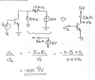
6. The transistor in the circuit below is biased at a dc collector current of 0.5 mA. What is the voltage gain?
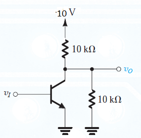
a) -1 V/V
b) -10 V/V
c) -100 V/V
d) -1000 V/V
View Answer
Explanation:
7. For a BJt Vt is 5 V, Rc = 1000 ohm and bias current Ic is 12 mA. The value of the voltage gain is __________
a) -1.2 V/V
b) -2.4 V/V
c) -3.6 V/V
d) -4.8 V/V
View Answer
Explanation: Voltage gain is (Ic X Rc) / Vt.
8. For the BJT amplifier circuit with Vcc = +10 V, Rc = 1 kΩ and the DC collector bias current equal to 5 mA. The value of the voltage gain is _______________
a) -2 V/V
b) -4 V/V
c) -10 V/V
d) -20 V/V
View Answer
Explanation: The voltage is 400 X Ic where Ic is 5 mA.
9. For the BJT amplifier circuit with Vcc = +10 V, Rc = 1 kΩ and the DC collector bias current equal to 5 mA. The maximum possible positive output signal swing as determined by the need to keep the transistor in the active region.
a) -1.7 V
b) -2.7 V
c) -3.7 V
d) -4.7 V
View Answer
Explanation: The maximum voltage swing is given by -10 + 0.3 + (Ic X Rc). Putting Ic as 5 mA, we get -4.7 mV.
10. For the BJT amplifier circuit with Vcc = +10 V, Rc = 1 kΩ and the DC collector bias current equal to 5 mA. The maximum possible negative output signal swing as determined by the need to keep the transistor in the active region.
a) 0.5 V
b) 1 V
c) 5 V
d) 10 V
View Answer
Explanation: It is given by -10 + 10 + (Ic X Rc). Putting Ic as 5 mA we get 5V.
Sanfoundry Global Education & Learning Series – Electronic Devices and Circuits.
To practice all areas of Electronic Devices and Circuits, here is complete set of 1000+ Multiple Choice Questions and Answers.
If you find a mistake in question / option / answer, kindly take a screenshot and email to [email protected]
