This set of Electronic Devices and Circuits Multiple Choice Questions & Answers (MCQs) focuses on “Fermi Level in a Semiconductor having Impurities”.
1. Which states get filled in the conduction band when the donor-type impurity is added to a crystal?
a) Na
b) Nd
c) N
d) P
View Answer
Explanation: When the donor-type impurity is added to a crystal, first Nd states get filled because it is of the highest energy.
2. Which of the following expression represent the correct formulae for calculating the exact position of the Fermi level for p-type material?
a) EF = EV + kTln(ND / NA )
b) EF = -EV + kTln(ND / NA )
c) EF = EV – kTln(ND / NA )
d) EF = -EV – kTln(ND / NA )
View Answer
Explanation: The correct position of the Fermi level is found with the formula in the ‘a’ option.
3. Where will be the position of the Fermi level of the n-type material when ND=NA?
a) Ec
b) Ev
c) Ef
d) Efi
View Answer
Explanation: When ND=NA, kTln(ND/NA )=0
So,
Ef=Ec.
4. When the temperature of either n-type or p-type increases, determine the movement of the position of the Fermi energy level?
a) Towards up of energy gap
b) Towards down of energy gap
c) Towards centre of energy gap
d) Towards out of page
View Answer
Explanation: whenever the temperature increases, the Fermi energy level tends to move at the centre of the energy gap.
5. Is it true, when the temperature rises, the electrons in the conduction band becomes greater than the donor atoms?
a) True
b) False
View Answer
Explanation: When the temperature increases, there is an increase in the electron-hole pairs and all the donor atoms get ionized, so now the thermally generated electrons will be greater than the donor atoms.
6. If the excess carriers are created in the semiconductor, then identify the correct energy level diagram.
a) 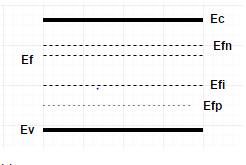
b) 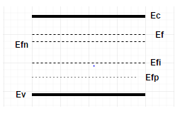
c) 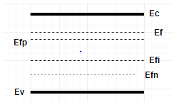
d) 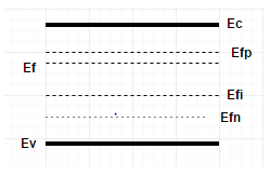
View Answer
Explanation: The diagram A refers the most suitable energy level diagrams because Efp>Ef>Efi>Efp>Ev.
7. If excess charge carriers are created in the semiconductor then the new Fermi level is known as Quasi-Fermi level. Is it true?
a) True
b) False
View Answer
Explanation: Quasi-fermi level is defined as the change in the level of the Fermi level when the excess chare carriers are added to the semiconductor.
8. Ef lies in the middle of the energy level indicates the unequal concentration of the holes and the electrons?
a) True
b) False
View Answer
Explanation: When the Ef is in the middle of the energy level, it indicates the equal concentration of the holes and electrons.
9. Consider a bar of silicon having carrier concentration n0=1015 cm-3 and ni=1010cm-3. Assume the excess carrier concentrations to be n=1013cm-3, calculate the quasi-fermi energy level at T=300K?
a) 0.2982 eV
b) 0.2984 eV
c) 0.5971 eV
d) 1Ev
View Answer
Explanation:
=1.38*10-23*300*ln(1013+1015/1013)
=0.2984 eV.
10. Consider a bar of silicon having carrier concentration n0=1015 cm-3, ni=1010cm-3 and p0=105cm-3. Calculate the quasi-fermi energy level in eV?
a) 0.1985
b) 0.15
c) 0.1792
d) 0.1
View Answer
Explanation: Using the same equation,
Substituting the respective values,
EFi – EFp=0.1792 eV.
Sanfoundry Global Education & Learning Series – Electronic Devices and Circuits.
To practice all areas of Electronic Devices and Circuits, here is complete set of 1000+ Multiple Choice Questions and Answers.
If you find a mistake in question / option / answer, kindly take a screenshot and email to [email protected]
