This set of Tricky Electronic Devices and Circuits Questions and Answers focuses on “MOSFET in Small Signal Operation”.
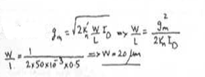
1. An NMOS technology has μnCox = 50 μA/V2 and Vt = 0.7 V. For a transistor with L = 1μm, find the value of W that results in gm 1mA/V at ID = 0.5 mA.
a) 10 μm
b) 20 μm
c) 30 μm
d) 40 μm
View Answer
Explanation:
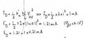
2. Consider an NMOS transistor having kn= 2 mA/V2. Let the transistor be biased at VOV = 1V. For operation in saturation, what dc bias current ID results? If a +0.1-V signal is superimposed on VGS, find the corresponding increment in collector current by evaluating the total collector current ID and subtracting the dc bias current ID.
a) ID = 1mA and Increment = 0.21 mA
b) ID = 1mA and Increment = 0.42 mA
c) ID = 2mA and Increment = 0.21 mA
d) ID = 2mA and Increment = 0.42 mA
View Answer
Explanation:
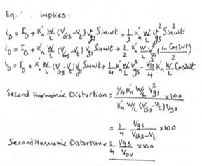
3. We know ID =1/2 kn (VGS + vgs – Vt)2. Let the signal vgs be a sine wave with amplitude Vgs, and substitute vgs = Vgs sin ω t in Eq.(5.43). Using the trigonometric identity show that the ratio of the signal at frequency 2ω to that at frequency ω , expressed as a percentage (known as the second-harmonic distortion) is
a) Vgs/Vov x 100%
b) 1/2Vgs/Vov x 100%
c) 1/4Vgs/Vov x 100%
d) 1/8Vgs/Vov x 100%
View Answer
Explanation:
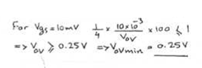
4. If in a particular application Vgs is 10 mV, find the minimum overdrive voltage at which the transistor should be operated so that the second-harmonic distortion is kept to less than 1%.
a) 1V
b) 0.75V
c) 0.5V
d) 0.25V
View Answer
Explanation:
5. An NMOS amplifier is to be designed to provide a 0.50-V peak output signal across a 50-kΩ load that can be used as a drain resistor. If a gain of at least 5 V/V is needed, what value of gm is required?
a) 0.1 mA/V
b) 0.2 mA/V
c) 0.4 mA/V
d) 0.8 mA/V
View Answer
Explanation: gmRd = 5 or gm= 5/50 mA/V.
6. An NMOS amplifier is to be designed to provide a 0.50-V peak output signal across a 50-kΩ load that can be used as a drain resistor. Using a dc supply of 3 V, what values of ID and VOV would you choose?
a) 0.34 mA and 0.35 V respectively
b) 0.34 mA and 0.69 V respectively
c) 0.034 mA and 0.35 V respectively
d) 0.034 mA and 0.69 V respectively
View Answer
Explanation:
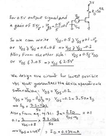
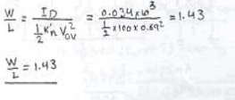
7. An NMOS amplifier is to be designed to provide a 0.50-V peak output signal across a 50-kΩ load that can be used as a drain resistor. What W/L ratio is required if μnCox = 200 μA/V2?
a) 1.23
b) 1.23
c) 1.43
d) 1.53
View Answer
Explanation:
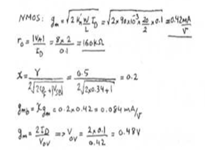
8. For a 0.8-μm CMOS fabrication process: Vtn= 0.8 V, Vtp = −0.9 V, μnCox = 90 μA/V2, μpCox = 30 μA/V2, Cox = 1.9 fF/μm2, VA (n-channel devices) = 8L (μm), and |VA| (p-channel devices) = 12L (μm). Find the small-signal model parameters (gm, ro and gmb) for an NMOS transistor having W/L = 20 μm/2 μm and operating at ID = 100 μA and |VSB| = 1V.
a) gm= 0.42mA/V, ro= 160 kΩ, gmb = 0.084 mA/V
b) gm= 0.21mA/V, ro= 160 kΩ, gmb= 0.042 mA/V
c) gm= 0.42mA/V, ro= 80 kΩ, gmb = 0.042 mA/V
d) gm= 0.24mA/V, ro= 80 kΩ, gmb = 0.084 mA/V
View Answer
Explanation:
9. For a 0.8-μm CMOS fabrication process: Vtn= 0.8 V, Vtp = −0.9 V, μnCox = 90 μA/V2, μpCox = 30 μA/V2, Cox = 1.9 fF/μm2, VA (n-channel devices) = 8L (μm), and |VA| (p-channel devices) = 12L (μm). Find the small-signal model parameters (gm, ro and gmb) for a PMOS transistor having W/L = 20 μm/2 μm and operating at ID = 100 μA and |VSB| = 1V.
a) gm= 0.24mA/V, ro= 240 kΩ, gmb = 0.024 mA/V
b) gm= 0.24mA/V, ro= 120 kΩ, gmb = 0.048 mA/V
c) gm= 0.24mA/V, ro=240 kΩ, gmb = 0.048 mA/V
d) gm= 0.12mA/V, ro= 240 kΩ, gmb = 0.048 mA/V
View Answer
Explanation:
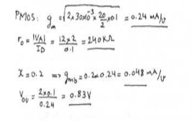
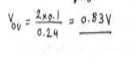
10. The overdrive voltage at which each device must be operating is
a) NMOS = 0.83V and PMOS = 0.48V
b) NMOS = 0.48V and PMOS = 0.83V
c) NMOS = 0.24V and PMOS = 0.41V
d) NMOS = 0.41V and PMOS = 0.24V
View Answer
Explanation:
NMOS case
PMOS case
Sanfoundry Global Education & Learning Series – Electronic Devices and Circuits.
To practice Tricky questions and answers on all areas of Electronic Devices and Circuits, here is complete set of 1000+ Multiple Choice Questions and Answers.
If you find a mistake in question / option / answer, kindly take a screenshot and email to [email protected]
