This set of Electronic Devices and Circuits Assessment Questions and Answers focuses on “Problems on AC and DC Analysis”.
1. In the circuit, transistor has β =60, VBE=0.7V. Find the collector to emitter voltage drop hoe.
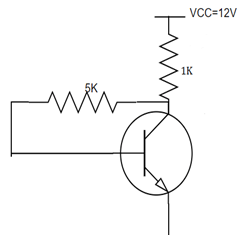
a) 5V
b) 3V
c) 8V
d) 6V
View Answer
Explanation: We know, IC=(VCC-VBE)/RB
By putting the values, we have IC=5.9mA. IE=IC/α. So, IE=5.99mA.
hoe= VCC-RC(IC+IB). We have hoe=6V.
2. For the circuit shown, find the quiescent point.
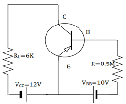
a) (6V, 1mA)
b) (4V, 10mA)
c) (10V, 3mA)
d) (3mA, 10V)
View Answer
Explanation: We know, hoe=12V
(IC)SAT =VCC/RL=12/6K=2mA. IB=10V/0.5M=20µA. IC= βIB=1mA. I
hoe=VCC-ICRL=12-1*6=6V. So, quiescent point is (6V, 1mA).
3. For the circuit shown, find the quiescent point.
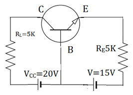
a) (10V, 4mA)
b) (4V, 10mA)
c) (10V, 3mA)
d) (3mA, 10V)
View Answer
Explanation: We know, IE=VEE/RE=10/5kΩ=2mA
IC=α IE =IE =2mA
VCB=VCC-ICRL=20-10=10V. So, quiescent point is (10V, 2mA).
4. In the circuit shown below, β =100 and VBE=0.7V. The Zener diode has a breakdown voltage of 6V. Find the operating point.
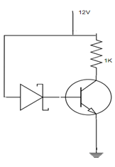
a) (6.7V, 5.3mA)
b) (5.7V, 5.3mA)
c) (6.7V, 5mA)
d) (6V, 5mA)
View Answer
Explanation: We know, by KVL -12+(IC+IB)1K+6+VBE=0
We have IE=5.3. IC= αIE=5.24mA. From another loop, -12+IEIK+VBE=0
We have, hoe=12-5.3m*1000=6.7V. Hence the Q point is (6.7V, 5.3mA).
5. When the β value is large for a given transistor, the IC and hoe values are given by_________
a) (VCC-VBE)/RB, VCC-RCIC
b) (VCC+VBE)/RB, VCC-RC(IC+IB)
c) (VCC+VBE)/RB, VCC+RC(IC+IB)
d) (VCC+VBE)/RB,VCC+RC(IC-IB)
View Answer
Explanation: The base current IB is zero when β value is large. So, the hoe changes to VCC-RCIC. The collector current IC is changed to (VCC-VBE)/RB from β(VCC-VBE)/(1+ β)RE+ RB.
6. For the circuit shown, find the quiescent point.
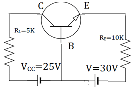
a) (10V, 4mA)
b) (4V, 10mA)
c) (10V, 3mA)
d) (3mA, 10V)
View Answer
Explanation: We know, IE=VEE/RE=30/10kΩ=3mA
IC=α IE =IE =3mA
VCB=VCC-ICRL=25-15=10V. So, quiescent point is (10V, 3mA).
7. The PNP transistor when used for switching the power, then it is called_________
a) sourcing current
b) sinking current
c) forward sourcing
d) reverse sinking
View Answer
Explanation: Sometimes DC current gain of a bipolar transistor is too low to directly switch the load current or voltage, so multiple switching transistors is used. The load is connected to ground and the transistor switches the power to it.
8. In which of the regions, the small capacitors are open circuited?
a) high frequency
b) medium frequency
c) low frequency
d) the region does not affect he capacitors
View Answer
Explanation: In low frequency region, the small capacitors are open circuited and large capacitors are in active state. In high frequency region, the large capacitors are short circuited and small capacitors are active.
9. In mid frequency region, the large capacitors are short and small capacitors are open circuited. What happens to the RC coupled circuit?
a) the circuit is now frequency blind
b) it is DC isolated
c) the circuit turns reactive
d) the circuit is AC dependent
View Answer
Explanation: In the mid frequency region, the whole circuit is resistive because the large capacitors are short and small capacitors are open circuited. The gain is constant in this region. So, the circuit is frequency blind as the gain is constant in this region.
10. In low frequency region, the gain_________
a) increases
b) decreases
c) remains same
d) depends on value of capacitors
View Answer
Explanation: At very low frequency, the gain decreases due to the coupling capacitor. When the frequency is decreased, the reactance of the circuit increases and the drop across the coupling capacitor increases. The gain is therefore decreased as the output decreased.
Sanfoundry Global Education & Learning Series – Electronic Devices and Circuits.
To practice all areas of Electronic Devices and Circuits Assessment Questions, here is complete set of 1000+ Multiple Choice Questions and Answers.
If you find a mistake in question / option / answer, kindly take a screenshot and email to [email protected]
