This set of Electronic Devices and Circuits Quiz focuses on “DC Imperfections in Operational Amplifiers”.
1. Consider an inverting amplifier with a nominal gain of 1000 constructed from an op amp with an input offset voltage of 3 mV and with output saturation levels of ±10 V. What is (approximately) the peak sine-wave input signal that can be applied without output clipping?
a) 7 mV
b) 10 mV
c) 13 mV
d) 9mV
View Answer
Explanation: The maximum that can be sent without clipping is 10V – 1000 X 3mV or 7V.
2. Consider an inverting amplifier with a nominal gain of 1000 constructed from an op amp with an input offset voltage of 3 mV and with output saturation levels of ±10 V. If the effect of VOs(input offset voltage) is nulled at room temperature (250C), how large an input can one now apply if the circuit is to operate at a constant temperature?
a) 8.5 mV
b) 9 mV
c) 9.5 mV
d) 10 mV
View Answer
Explanation: Explanation: Maximum signal that will not be clipped is 10mV because 10mV X 1000 = 10V.
3. Consider an inverting amplifier with a nominal gain of 1000 constructed from an op amp with an input offset voltage of 3 mV and with output saturation levels of ±10 V. If the effect of VOs(input offset voltage) is nulled at room temperature (250C). The circuit is to operate at a temperature in the range 0°C to 75°C and the temperature coefficient of VOS is 10 μV/°C?
a) 8.5 mV
b) 9 mV
c) 9.5 mV
d) 10 mV
View Answer
Explanation: Since the effect is nullified at 25oC, the peak that can be sent now is given by 10 – (75-25) X 0.1 mV.
4. One of the DC imperfections of the amplifiers are dc offset voltage which is
a) Existence of output signal even when the common mode signal is zero
b) Existence of common mode signal causing zero output signal
c) Existence of output signal even when the differential signal is zero
d) Existence of differential signal causing zero output signal
View Answer
Explanation: DC offset voltage is existence of output signal even when the differential signal is zero.
5. For the amplifier shown determine the value of the bias current (Ib) and input offset current (Io) respectively.
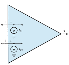
a) Ib = IB1 + IB2 Io = IB1 – IB2
b) Ib = IB1 + IB2 Io = | IB1 – IB2 |
c) Ib = 0.5(IB1 + IB2) Io = | IB1 – IB2 |
d) Ib = 0.5(IB1 + IB2) Io = IB1 – IB2
View Answer
Explanation: Standard mathematical expressions are used with the given variables.
6. Consider the circuit shown below which reduces the impact of the input bias current. If IB1 = IB2 = Input bias current, then determine the value of R3 so that the output voltage (v0) is not impacted by the input bias current.
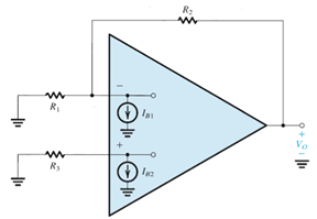
a) (R1 R2)/(R1+R2)
b) (R1 R2)/(R1-R2)
c) R1-(R1 R2)/(R1+R2)
d) R2- (R1 R2)/(R1+R2)
View Answer
Explanation: This will be possible when R3 has the same value as the net effect of R1 and R2.
7. Consider an inverting amplifier circuit designed using an op amp and two resistors, R1 = 10 kΩ and R2 = 1 MΩ. If the op amp is specified to have an input bias current of 100 nA and an input offset current of 10 nA, find the output dc offset voltage resulting.
a) 0.1 mV
b) 1 mV
c) 10 mV
d) 100 mV
View Answer
Explanation: Use the mathematical definition of bias current and offset current.
8. Consider a Miller integrator with a time constant of 1ms and an input resistance of 10 kΩ. Let the op amp have VOS (offset voltage) = 2 mV and output saturation voltages of ±12 V. Assuming that when the power supply is turned on the capacitor voltage is zero, how long does it take for the amplifier to saturate?
a) 3s
b) 6s
c) 9s
d) 12s
View Answer
Explanation: Use vO = VOS
(VOS/CR)t.
9. Consider a Miller integrator with a time constant of 1ms and an input resistance of 10 kΩ. Let the op amp have VOS (offset voltage) = 2 mV and output saturation voltages of ±12 V. Select the largest possible value for a feedback resistor RF so that at least ±10 V of output signal swing remains available.
a) 10 kΩ
b) 100 kΩ
c) 1 MΩ
d) 10 MΩ
View Answer
Explanation: Use vO = VOS
(VOS/CR)t.
10. Consider a Miller integrator with a time constant of 1ms and an input resistance of 10 kΩ. Let the op amp have VOS (offset voltage) = 2 mV and output saturation voltages of ±12 V. What is the corner frequency of the resulting STC network?
a) 1 Hz
b) 0.16 Hz
c) 0.33 Hz
d) 0.5 Hz
View Answer
Explanation: The required answer is given by 1/6 Hz.
Sanfoundry Global Education & Learning Series – Electronic Devices and Circuits.
To practice all areas of Electronic Devices and Circuits for Quizzes, here is complete set of 1000+ Multiple Choice Questions and Answers.
If you find a mistake in question / option / answer, kindly take a screenshot and email to [email protected]
