This set of Advanced Electronic Devices and Circuits Questions and Answers focuses on “Discrete-Circuit MOS Amplifiers”.
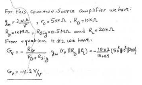
1. Calculate the overall voltage gain Gv of a common source amplifier for which gm = 2mA/V, RD = 10 kΩ, R0 = 10 kΩ and RG = 10 MΩ. The amplifier is fed from a signal source of Thevenin resistance of 0.5MΩ and the amplifier is coupled with a load of 10 kΩ.
a) -11.2 V/V
b) -22.4 V/V
c) -33.6 V/V
d) -44.8 V/V
View Answer
Explanation:
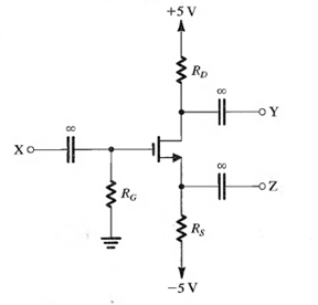
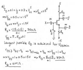
2. The MOSFET circuit below has Vt = 1V, knW/L = 0.8 mA/V2 and VA = 40V. Find the value of RG so that iD = 0.1 mA, the largest possible value of RD is used while the maximum signal swing at the drain is of 1V and the input resistance at the gate is 10 MΩ.
a) 1 MΩ
b) 10 MΩ
c) 0.1 MΩ
d) 0.01 MΩ
View Answer
Explanation:
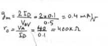
3. The MOSFET circuit below has Vt = 1V, knW/L = 0.8 mA/V2 and VA = 40V. Find the value of gm at the bias point.
a) 0.1 mA/V
b) 0.2 mA/V
c) .0.3 mA/V
d) 0.4 mA/V
View Answer
Explanation:
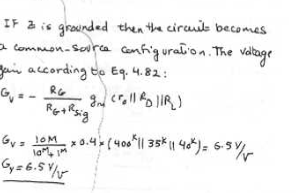
4. The MOSFET circuit below has Vt = 1V, knW/L = 0.8 mA/V2 and VA = 40V. If terminal Z is grounded, X is connected to a signal source having a resistance of 1 MΩ and terminal Y is connected to a load resistance of 40 kΩ, find the voltage gain from the signal source to the load.
a) 3.25 v/V
b) 6.5 V/V
c) 9.75 V/V
d) 13 V/V
View Answer
Explanation:
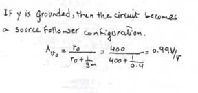
5. The MOSFET circuit below has Vt = 1V, knW/L = 0.8 mA/V2 and VA = 40V. If terminal Y is grounded find the voltage gain from X to Z with Z open-circuit.
a) 0.33 V/V
b) 0.66 V/V
c) 0.99 V/V
d) None of the mentioned
View Answer
Explanation:
6. The MOSFET circuit below has Vt = 1V, knW/L = 0.8 mA/V2 and VA = 40V. If terminal X is grounded and terminal Z is connected to a current source delivering a current of 10 µA and having a resistance of 100 kΩ, find the voltage signal that can be measured at Y neglecting the effect of V0.
a) 0.34V
b) 0.68 V
c) 3.4 V
d) 6.8 V
View Answer
Explanation:

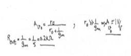
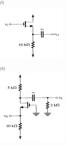
7. The NMOS transistor in source follower circuit shown has gm = 5mA/V and a large r0. Find the output resistance.
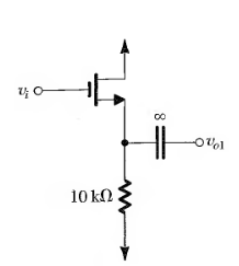
a) 0.1 kΩ
b) 0.2 kΩ
c) 0.3 kΩ
d) 0.4 kΩ
View Answer
Explanation:

8. The NMOS transistor in source follower circuit shown has gm = 5mA/V and a large r0. Find the open-Circuit voltage gain.
a) 1 V/V
b) 2 V/V
c) 3 V/V
d) 4 V/V
View Answer
Explanation:
9. The NMOS transistor in the common gate amplifier as shown in the circuit below has gm = 5 mA/V. Find the input resistance and the voltage gain.
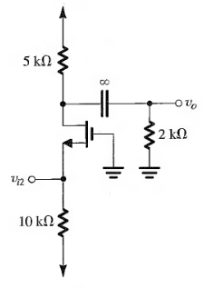
a) Input resistance: 0.1 kΩ and Voltage gain: 3.05 V/V
b) Input resistance: 0.1 kΩ and Voltage gain: 3.05 V/V
c) Input resistance: 0.2 kΩ and Voltage gain: 3.05 V/V
d) Input resistance: 0.2 kΩ and Voltage gain: 7.1 V/V
View Answer
Explanation:
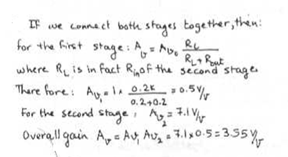
10. If the output of the source follower in (I) is connected to the input of the common gate amplifier of (II). Determine the overall voltage gain (V0 /Vi).
a) 1.55 V/V
b) 3.55 V/V
c) 5.55 V/V
d) 7.55 V/V
View Answer
Explanation:
Sanfoundry Global Education & Learning Series – Electronic Devices and Circuits.
To practice Advanced questions and answers on all areas of Electronic Devices and Circuits, here is complete set of 1000+ Multiple Choice Questions and Answers.
If you find a mistake in question / option / answer, kindly take a screenshot and email to [email protected]
