This set of Electronic Devices and Circuits online test focuses on “Quantitative Theory of the P-N diode Currents”.
1. What is the thickness of ‘space charge region’ or ‘transition region’ in P-N junction diode?
a) 1 micron
b) 5 micron
c) 10 micron
d) 2.876 micron
View Answer
Explanation: The region of the junction is depleted by mobile charges, hence it is called space charge region or depletion region or transition region which is 10-4 cm = 10-6 m= 1 micron.
2. If what of the following is doped into a semiconductor say germanium a P-N junction is formed.
a) Electrons and Protons
b) Protons and Neutrons
c) Neutrons and Electrons
d) Gallium and Phosphorus
View Answer
Explanation: A P-N junction is formed only when a donor impurities and acceptor impurities are added to either side of a semiconductor like silicon and germanium.
3. Which of the factors doesn’t change the diode current.
a) Temperature
b) External voltage applied to the diode
c) Boltzmann‘s constant
d) Resistance
View Answer
Explanation: I = Io [e(v/nVt) -1], as shown in this equation the diode current is dependent on temperature , voltage applied on the diode , Boltzmann’s constant but diode current is not dependent on resistance as it is independent of resistance.
4. The product of mobility of the charge carriers and applied Electric field intensity is known as
a) Drain velocity
b) Drift velocity
c) Push velocity
d) Pull velocity
View Answer
Explanation: When the semiconductors like silicon and germanium is implied by an electric field the charge carriers when get drifted by certain velocity known as drift velocity. Drift velocity is product of mobility of charge carriers and field intensity.
5. The tendency of charge carriers to move from a region of heavily concentrated charges to region of less concentrated charge is known as.
a) Depletion current
b) Drain current
c) Diffusion current
d) Saturation current
View Answer
Explanation: In a semiconductor the charge will always have a tendency to move from higher concentrated area to less concentrated area to maintain equilibrium this movement of charges will result in diffusion current.
6. If the drift current is 100mA and diffusion current is 1A what is the total current in the semiconductor diode.
a) 1.01 A
b) 1.1 A
c) 900m A
d) 10 A
View Answer
Explanation: We know that the total current in a semiconductor is equal to sum of both drift current and diffusion current. Total current = 1A + 100mA =1.1A.
7. Which of the following is reverse biased?
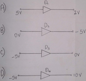
a) A)
b) B)
c) C)
d) D)
View Answer
Explanation: The P-N junction diode is forward bias when the voltage applied to p type is greater than the n type and vice versa, since the voltage applied to p type is less in C) it is the answer.
8. The drift velocity is 5V and the applied electric field intensity 20v/m what will be the mobility of charge carriers.
a) 100 m2/ (vs)
b) 4 m2/ (vs)
c) 15 m2/ (vs)
d) 0.25 m2/ (vs)
View Answer
Explanation: We know that mobility of charge carriers is drift velocity divide by applied electric field intensity. Mobility = drift velocity / field intensity.
9. When there is an open circuit what will be the net hole current.
a) 5A
b) 0.05A
c) 0.5A
d) 0A
View Answer
Explanation: If there is any current present under open circuit there will be an indefinite growth of holes at one end of the semiconductor which is practically not possible hence zero amperes.
10. Rate of change of concentration per unit length in a semiconductor is called as.
a) Concentration change
b) Concentration mixture
c) Concentration gradient
d) Concentration variant
View Answer
Explanation: In a semiconductor the holes as well as electrons which are the charge carriers is not equally concentrated on all regions of the semiconductor the change in their rate is referred as concentration gradient.
Sanfoundry Global Education & Learning Series – Electronic Devices and Circuits.
To practice all areas of Electronic Devices and Circuits for online tests, here is complete set of 1000+ Multiple Choice Questions and Answers.
If you find a mistake in question / option / answer, kindly take a screenshot and email to [email protected]
