This set of Linear Integrated Circuit Multiple Choice Questions & Answers (MCQs) focuses on “Clippers and Clampers”.
1. Which circuit is used for obtaining desired output waveform in operational amplifier?
a) Clipper
b) Clamper
c) Peak amplifier
d) Sample and hold
View Answer
Explanation: In an op-amp clipper circuits a rectifier diode is used to clip off certain portions of the input signal to obtain a designed output waveform.
2. The clipping level in op-amp is determined by
a) AC supply voltage
b) Control voltage
c) Reference voltage
d) Input voltage
View Answer
Explanation: The clipping level is determined by the reference voltage which should be less than the input voltage range of an op-amp.
3. In a positive clipper, the diode conducts when
a) Vin < Vref
b) Vin = Vref
c) Vin > Vref
d) None of the mentioned
View Answer
Explanation:In a positive clipper, the diode conducts until Vin = Vref (during the positive half cycle of the input), because when Vin < Vref, the voltage (Vref) at the negative input is higher than that at the positive input.
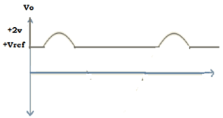
4. What happens if the potentiometer Rp is connected to negative supply?
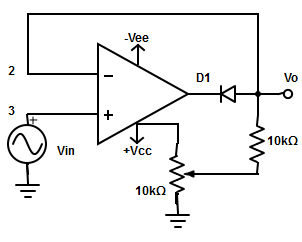
a) Output waveform below -Vref will be clipped off
b) Output waveform above +Vref will be clipped off
c) Output waveform above -Vref will be clipped off
d) Output waveform below +Vref will be clipped off
View Answer
Explanation: If the potentiometer Rp is connected to negative supply -VEE instead of +VCC, the reference voltage Vref will be negative. As a result the entire output waveform above -Vref to be clipped off.
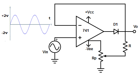
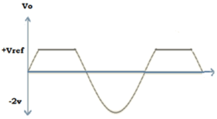
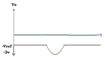
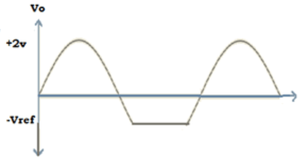
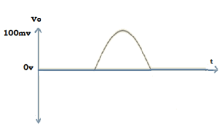
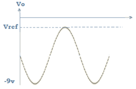
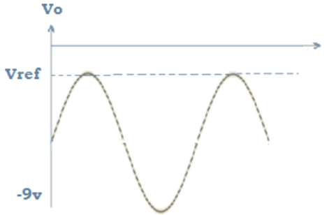
5. Find the output waveform for when Vin < Vref
a)
b)
c)
d)
View Answer
Explanation: The negative portion of the output voltage below -Vref is clipped off because, diode will be in off condition when Vin < Vref.
6. What happens if the input voltage is higher than reference voltage in a positive clipper?
a) Output voltage = Reference voltage
b) Output voltage = DC Positive voltage
c) Output voltage = Input voltage
d) All of the mentioned
View Answer
Explanation: When input voltage is higher than reference voltage, the op-amp operates in open loop and diode become reverse biased. Thus, the output voltage will be equal to reference voltage.
7. A positive small signal halfwave rectifier can
a) Rectify signals with peak value only
b) Rectify signals with value of few millivolts only
c) Rectify signals with both peak value and down to few millivolts
d) None of the mentioned
View Answer
Explanation: A positive small signal halfwave rectifier can rectify signals with peak values down to few millivolts, because the high open loop gain of the op-amp automatically adjusts the voltage drive to the diode, so that the rectified output peak is the same as the input.
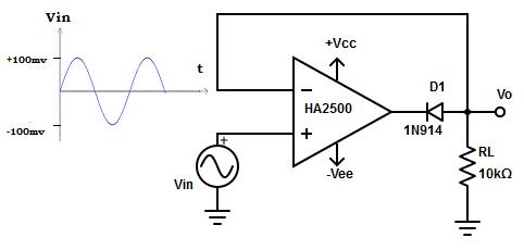
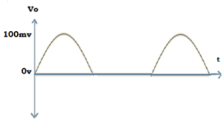
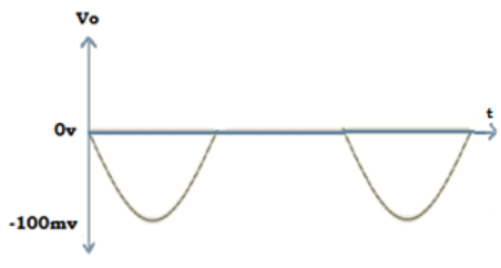
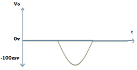
8. Determine the output waveform of negative small signal half wave rectifier.
a)
b)
c)
d)
View Answer
Explanation: During the positive alteration of Vin, D1 is reverse biased. Therefore, Vo =0v. On the other hand, during the negative alteration, D1 is forward biased and hence Vo follows Vin.
9. Diode in small signal positive halfwave rectifier circuit acts as
a) Ideal diode
b) Clipper diode
c) Clamper diode
d) Rectifier diode
View Answer
Explanation: The diode acts as an ideal diode, since the voltage across the ON diode is divided by the open loop gain of the op-amp. As the input voltage starts increasing in the positive direction, the output of the op-amp also increases positively till the diode become forward biased.
10. How to minimize the response time and increase the operating frequency range of the op-amp?
a) Positive halfwave rectifier with two diodes
b) Positive halfwave rectifier with one diode
c) Negative halfwave rectifier with two diodes
d) Negative halfwave rectifier with one diode
View Answer
Explanation: Negative halfwave rectifier circuit with two diodes are used so that the output of the op-amp does not saturate. Thus, minimizes the response time and increases the operating frequency range.
11. Why a voltage follower stage is connected at the output of the negative small signal half wave rectifier?
a) Due to Non-uniform input resistance
b) Due to Non-uniform output resistance
c) Due to Uniform output voltage
d) None of the mentioned
View Answer
Explanation: The output resistance of the circuit is non-uniform as it depends on the state of diode. That is, the output impedance is low when diode is on and high when diode is off.
12. A circuit with a predetermined dc level is added to the output voltage of the op-amp is called
a) Clamper
b) Positive clipper
c) Halfwave rectifier
d) None of the mentioned
View Answer
Explanation: A clamper clamps the output to a desired dc level.
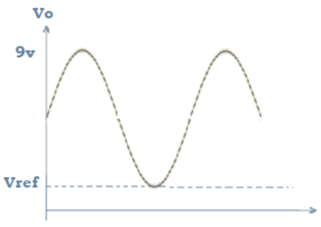
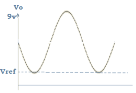
13. Determine the output waveform for a peak amplifier with input =4Vpsinewave and Vref=1V.
a)
b)
c)
d)
View Answer
Explanation: In a peak amplifier the input waveform peak is clamped at Vref.
The output voltage Vo=2Vp+Vref=(2×4v)+1v = 9v.
14. An op-amp clamper circuit is also referred as
a) DC cutter
b) DC inserter
c) DC lifter
d) DC leveller
View Answer
Explanation: In an op-amp clamper circuit, a pre-determined dc level is deliberately inserted at the output voltage. For this reason, the clamper is sometimes called as DC inserter.
15. At what values of Ci and Rd a precision clamping can obtained in peak clamper when the time period of the input waveform is 0.4s?
a) Ci=0.1µF and Rd=10kΩ
b) Ci=0.47µF and Rd=10kΩ
c) Ci=33µF and Rd=10kΩ
d) Ci=2.5µF and Rd=10kΩ
View Answer
Explanation: For precision clamping, Ci and Rd << T/2. So, (0.1µF×10 kΩ) << (0.4/2) = 1×10⁻³ << 0.2. Therefore, Ci=0.1µF and Rd=10kΩ.
Sanfoundry Global Education & Learning Series – Linear Integrated Circuits.
To practice all areas of Linear Integrated Circuits, here is complete set of 1000+ Multiple Choice Questions and Answers.
If you find a mistake in question / option / answer, kindly take a screenshot and email to [email protected]
- Apply for Electrical Engineering Internship
- Practice Electronics & Communication Engineering MCQs
- Practice Electrical Engineering MCQs
- Check Electrical Engineering Books
- Apply for Electronics & Communication Engineering Internship
