This set of Linear Integrated Circuit Interview Questions and Answers for freshers focuses on “Operational Amplifier Internal Circuit – 4”.
1. To increase the input resistance, the differential amplifier replaces transistor by
a) Current mirror
b) Current repeater
c) Darlington pair
d) All of the mentioned
View Answer
Explanation: Higher value of input resistance can be obtained by using Darlington pair in place of transistor.
2. In Darlington pair differential amplifier the current gain is given as 100. Where IB1=5µA and IC1=0.35mA. Determine IC2
a) 0.5mA
b) 1.5mA
c) 2mA
d) 0.15mA
View Answer
Explanation: The current gain in Darlington pair differential amplifier is given as β=( IC1+IC2)/IB1.
Substituting the values in the equation, we get
IC2=(β×IB1)-IC1 =(100×5µA)-0.35mA =0.15mA.
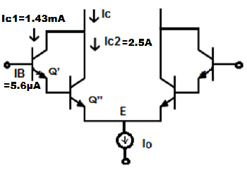
3. In the circuit shown, find the overall current gain?
a) 456218
b) 444878
c) 444210
d) 455734
View Answer
Explanation: From the circuit given, IB= IB1 = 5.6µA.
IE1= IB1+ IC1 = 1.43mA + 5.6µA = 1.435mA.
IE1= IB2 = 1.435mA.
The individual current gain values,
β1=IC1/ IB1
=> β1 = 1.43mA/5.6µA= 255.36.
Similarly,β2=IC2/ IB2
=> β2 = 2.5A / 1.435mA =1742.16
Therefore, the overall current gain, β = β1 × β2 = 255.36 × 1742.16 = 444878.
4. Introducing FET differential amplifier pair at the input stage of differential amplifier produces
a) High output resistance
b) High input resistance
c) Low input impedance
d) All of the mentioned
View Answer
Explanation: Input resistance of the order 1012 Ω is possible with JFET at the input stage of differential amplifier.
5. Why active load is used in amplifier to obtain large gain in intermediate stage of amplifier?
a) To obtain a very large voltage gain
b) To get High input resistance
c) To reduce the noises
d) To increase current gain
View Answer
Explanation: To increase gain usually large collector resistance value as gain is proportional to load resistor. However, due to limitation of maximum value load resistor, active loads are used in amplifier to obtain large gain in intermediate stages of amplifier.
6. Which circuit is used as active load for an amplifier
a) Wildar Current source
b) Darlington pair
c) Current Mirror
d) All of the mentioned
View Answer
Explanation: Current mirror has DC resistance (order of few kΩ), as quiescent voltage across it is a fraction of supply voltage and current in milliampere.
7. What is the equation of load current for a differential amplifier with an active load?
a) IL = gm×vd
b) IL = Iq /2
c) IL = β×Iq×( Vin1 – Vin2)
d) IL = 2×gm/( Vin1 – Vin2)
View Answer
Explanation: The load current is given as product of difference between input & output voltage and transconductance. Therefore, the equation of load current is ,
IL = gm×vd.
8. The input voltage of a difference amplifier are 2.5v and 4.9v. If the transconductance is 0.065Ω-1, determine the load current entering the next stage
a) 0.156A
b) 1.56A
c) 0.156mA
d) 15.6µA
View Answer
Explanation: Load current entering the next stages of amplifier is the sum of individual load current, which is given by IL = IL1+ IL2 (Since only two input voltages are given).
IL = gm×Vin1 + gm×Vin2
= gm×( Vin1 – Vin2) = 0.065 Ω-1×(4.9v-2.5v) = 0.156A.
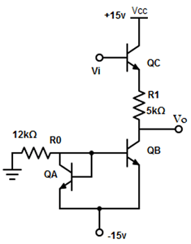
9. Calculate the VI – VO for the level shifter shown in the figure (Assume identical silicon transistor and very large value of β). Transistor QA and QB form current mirror.
a) 5.56V
b) 6.00v
c) 7.98v
d) 6.65v
View Answer
Explanation: Since the transistor QA and QB form current mirror, ICA= ICB = I.
=> I = (VCC – VBE) / R0 = (15v-0.7)/12k Ω (for β>>1, output current =input current)
=> I= 1.19mA.
The shift in level is given as VI – VO = VBE + I×R1 =0.07v+1.19mA×5kΩ =6.65v.
10. Load resistors (Re) is neglected for maximizing the voltage gain in amplifier because,
a) Requires large chip are
b) Requires large power supply
c) Quiescent drop across Re increases
d) All of the mentioned
View Answer
Explanation: As gain is proportional to load resistor, large resistance value is required. Due to limitation mentioned, it is neglected.
11. What is the need for level shifter in operational amplifier?
a) Level the quiescent voltage
b) Remove distortion at output
c) Limits the output voltage
d) Increase the quiescent voltage
View Answer
Explanation: Because of direct couple, Dc level rises stages to stage and tends to shift operating point. This limits output swing (Voltage).
12. Limitation of an output stage amplifier, if it emitter follower with complementary transistor
a) Cross-over distortion
b) Low impedance output
c) Shift in level
d) Active load current
View Answer
Explanation:The limitation in the amplifier is that , the output voltage remains zero until the input voltage exceeds cut in voltage VBE= 0.5v, which is known as cross-over distortion.
13. An output stage amplifier can produce output signal, when the input signal is
a) 0.48v
b) 0.9v
c) 1.2v
d) 0.5v
View Answer
Explanation: In an Output stage amplifier, due to cross-over distortion output voltage produces input voltage is greater than two times of cut-in voltage which is equal to 1v.
Since, VBE= 0.5v
=> 2×VBE= 1v.
14. Find the disadvantage in the following circuit diagram:
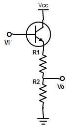
a) Voltage get attenuated by R1
b) Voltage get attenuated by R2
c) Voltage get attenuated by R1 and R2
d) Voltage shift get increased by the drop across R1 and R2
View Answer
Explanation: The output taken at the junction of R1 and R2 increases the voltage shift. However, the disadvantage is that, the signal voltage gets attenuated by R2.
=> R2/(R1 + R2).
Sanfoundry Global Education & Learning Series – Linear Integrated Circuits.
To practice all areas of Linear Integrated Circuit for Interviews, here is complete set of 1000+ Multiple Choice Questions and Answers.
If you find a mistake in question / option / answer, kindly take a screenshot and email to [email protected]
