This set of Linear Integrated Circuit Multiple Choice Questions & Answers (MCQs) focuses on “Fabrication of FET”.
1. JFET is similar to that of fabrication of
a) Diode fabrication
b) BJT fabrication
c) FET fabrication
d) None of the mentioned
View Answer
Explanation: The basic processes used are as same as BJT fabrication. Epitaxial layer (collector of BJT) is used as the n-channel of JFET. The p+ is formed in n-channel by process of diffusion and n+ region formed under drain and source provide good ohmic contact.
2. What are the types of MOSFET devices available?
a) P-type enhancement type MOSFET
b) N-type enhancement type MOSFET
c) Depletion type MOSFET
d) All of the mentioned
View Answer
Explanation: MOSFET are available as Enhancement type and depletion type MOSFET. These are further classified into n-type and p-type device.
3. Which insulating layer used in Fabrication of MOSFET?
a) Aluminium oxide
b) Silicon Nitride
c) Silicon dioxide
d) None of the mentioned
View Answer
Explanation: Silicon dioxide is used as insulating layer in MOSFET Fabrication. It gives an extremely high input resistance in the order of 1010 to 1015 Ω for MOSFET.
4. Which of the following plays an important role in improving device performance of MOSFET?
a) Dielectric constant
b) Threshold voltage
c) Power supply voltage
d) Gate to drain voltage
View Answer
Explanation: In MOSFET, the threshold voltage is typically 3 to 6v. This large voltage is not compatible with 5v supply used in digital IC. So, to improve device performance, magnitude of threshold voltage should be reduced.
5. A technique used to reduce the magnitude of threshold voltage of MOSFET?
a) Use of complementary MOSFET
b) Use of Silicon nitride
c) Using thin film technology
d) None of the mentioned
View Answer
Explanation: Silicon nitride is sandwiched between two SiO2 layer and provide necessary barrier .The dielectric constant of Si3N4 is 7.5, whereas that of SiO2 is 4. This increase in overall dielectric constant reduces threshold voltage.
6. Find the sequence of steps involved in fabrication of poly silicon gate MOSFET? 7. What is used to higher the speed of operation in MOSFET fabrication? 8. Why MOSFET is preferred over BJT in IC components? 9. Which of the following statement is true?
Step 1: Entire wafer surface of a Si3N4is coated and it is etched away with the help of mask to include source, gate and drain.
Step 2: The contact areas are defined using photolithographic process
Step3: Selective etching of Si3N4 and thin oxide growth
Step 4: Deposition of poly silicon gate
Step 5: thick oxide growth called field oxide and P
Step 6: Metallization and interconnection between substrate and source
a) 1->5->3->4->2->6
b) 1->3->4->2->5->6
c) 1->5->4->3->2->6
d) 1->4->2->5->3->6
View Answer
Explanation: The mentioned steps are the sequence of steps involved in the fabrication of poly silicon gate MOSFET.
a) Ceramic gate
b) Silicon dioxide
c) Silicon nitride
d) Poly silicon gate
View Answer
Explanation: In conventional metal gate, small overlap capacitance is present, which lowers the speed of operation. Due to self aligning property of poly silicon gate, it eliminates this capacitance.
a) MOSFET has low packing density
b) MOSFET has medium packing density
c) MOSFET has high packing density
d) MOSFET has no packing density
View Answer
Explanation: No isolation island is required in MOSFET structure because, the drain of an n-mos device is held positive with respect to source. This cutoff the drain to substrate diode and the source to substrate diode formed due to p+ region. In BJT, the isolation diffusion occupies extremely large percentage of chip area.
a) Fabrication of p-mos transistor require few additional steps compared to n-mos transistor
b) Fabrication of n-mos transistor require few additional steps compared to p-mos transistor
c) Fabrication on n-mos is same as that of p-mos transistor
d) Fabrication on n-mos is different from that of p-mos transistor
View Answer
Explanation: There are two additional steps required in the formation of p-mos transistor compared to n-mos transistor. Such as, the formation of n-region and ion implantation of p-type source and drain regions.
10. Find complementary MOSFET from the given circuit diagram?
a) 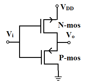
b) 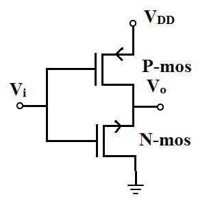
c) 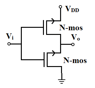
d) 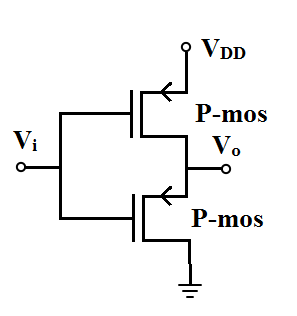
View Answer
Explanation: Complementary MOSFET is combination of n-mos and p-mos enhancement device such that the source of p-mos is connected to Vdd and source of n-mos is connected to ground.
Sanfoundry Global Education & Learning Series – Linear Integrated Circuits.
To practice all areas of Linear Integrated Circuits, here is complete set of 1000+ Multiple Choice Questions and Answers.
If you find a mistake in question / option / answer, kindly take a screenshot and email to [email protected]
