This set of Linear Integrated Circuit Multiple Choice Questions & Answers (MCQs) focuses on “High Frequency Op-Amp Equivalent Circuit”.
1. Which factor is responsible for the gain of the op-amp to roll-off after a certain frequency is reached
a) Capacitive effect
b) Resistive effect
c) Inductor effect
d) None of the mentioned
View Answer
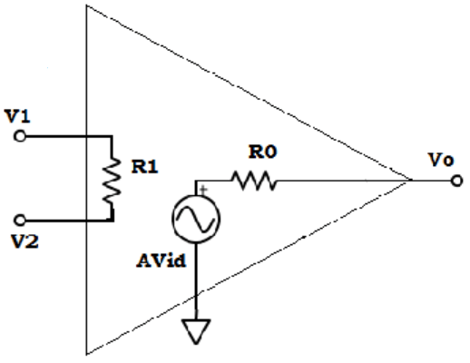
Explanation: The gain of the op-amp roll-off due to the presence of capacitive component, in the equivalent circuit of op-amp. The frequency increases as the reactance of the component decreases.
2. What remedy can be followed to maintain the operating frequency in the op-amps?
a) Use LC circuit
b) Use resistor
c) Use capacitor
d) Use transistor
View Answer
Explanation: Capacitors are used in the high frequency model of the op-amp at the output terminal to maintain or control the frequency.
3. How does the physical characteristic of semiconductor account for the increase in frequency of op-amps?
a) Transistor values
b) Junction capacitance
c) Dopant concentration
d) None of the mentioned
View Answer
Explanation: Op-amps are composed of BJTs and FETs which contain junction capacitors. These junction capacitors are very small and take finite values at higher frequency. So, when the reactances of these capacitors decrease, the frequency increases.
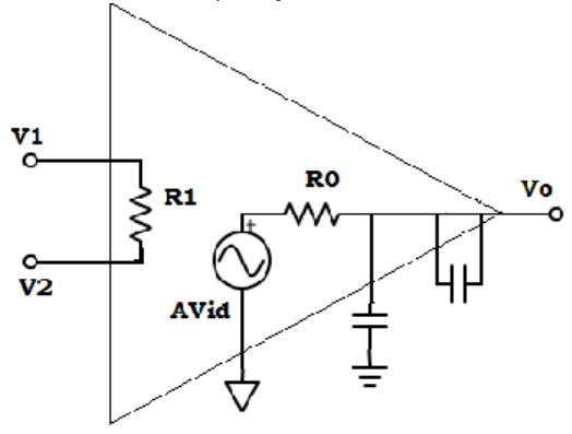
4. How are op-amp with three break frequency are represented
a) Using two capacitors
b) Using three capacitors
c) Using one capacitor
d) All of the mentioned
View Answer
Explanation: Op-amps with more than one break frequency may be represented by using as many capacitors as the break frequency they have.
5. In what way the internal construction of the op-amp contribute to capacitive effect in op-amp?
a) Formation of junction capacitor
b) Due to internally connected capacitors
c) Formation of stray capacitor
d) None of the mentioned
View Answer
Explanation: In op-amps a number of transistors, resistors and capacitors are integrated on the same substrate. In fact substrates act as an insulator and separate these components. So, the various components are connected by conducting paths. However, when two conducting paths are separated by an insulator, it acts as a capacitor (stray capacitor).
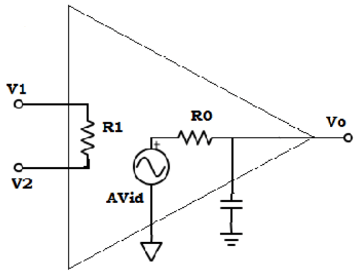
6. Determine the high frequency model op-amp with single break frequency
a)
b)
c)
d) None of the mentioned
View Answer
Explanation: Op-amp with only one break frequency is represented by adding a single capacitor at the output.
7. The gain of the differential amplifier is -125. Assume the voltage applied to bridge circuit Vdc=+10v and the unstrained resistance of four element of strain gage is 200Ω. When a certain weight is placed on the platform, the output voltage Vo=5v. Determine the change in resistance of each strain gage for analog weight scale. (Assuming the output is initially nulled).
a) 1Ω
b) 0.8Ω
c) 0.3Ω
d) 1.83Ω
View Answer
Explanation: The output voltage of analog weight scale, Vo = Vdc×(△R/R)×(RF/R1)
=> △R=( Vo/ Vdc)×(R1/RF)×R =( 5v×200Ω)/(125×10v) =0.8Ω.
8. Assume that the increase and decrease in the resistance of the strain gage element is by the same number of △R. Determine the unbalanced voltage equation.
a) V = – Vdc×(△R/R)
b) V = – Vdc×(△R/R+△R)
c) V = Vdc×(△R/R)
d) V = – Vdc×[(△R+ R)/R].
View Answer
Explanation: When the unstrained gage resistance are same, then the output voltage of the strain gage bridge circuit (unbalanced voltage) is given as V= -Vdc×(△R/R).
Sanfoundry Global Education & Learning Series – Linear Integrated Circuits.
To practice all areas of Linear Integrated Circuits, here is complete set of 1000+ Multiple Choice Questions and Answers.
If you find a mistake in question / option / answer, kindly take a screenshot and email to [email protected]
