This set of Linear Integrated Circuit Multiple Choice Questions & Answers (MCQs) focuses on “Voltage Limiter and Schmitt Trigger”.
1. Which circuit converts irregularly shaped waveform to regular shaped waveforms?
a) Schmitt trigger
b) Voltage limiter
c) Comparator
d) None of the mentioned
View Answer
Explanation: Schmitt trigger are also called as squaring circuit because, this type of circuit converts an irregularly shaped wave to a square wave or pulse.
2. Determine the upper and lower threshold voltage
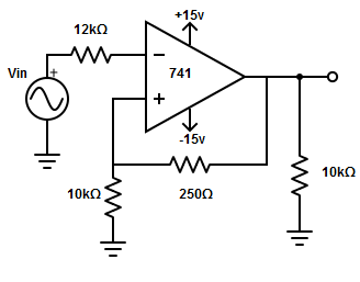
a) VUT = +14.63v, VLT= +14.63v
b) VUT = -14.63v, VLT= -14.63v
c) VUT = VLT= ±14.63v
d) None of the mentioned
View Answer
Explanation: Upper threshold voltage, VUT = [R1/(R1+ R2)]× (+Vsat) = [10kΩ/(10kΩ +250Ω)]×(+15v)= +14.63v.
Lower threshold voltage VLT = [R1/(R1+ R2)]×( -Vsat) = [10kΩ /(10kΩ+250Ω)]×(-15v)= -14.63v.
3. What happens if the threshold voltages are made longer than the noise voltages in schmitt trigger?
a) All the mentioned
b) Enhance the output signal
c) Reduce the transition effect
d) Eliminate false output transition
View Answer
Explanation: In schmitt trigger, if the threshold voltage VUT and VLT are made larger than the input noise voltage. The positive feedback will eliminate the false output transition.
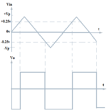
4. To a schmitt trigger in non-inverting configuration an input triangular wave of 1Vp is applied. What will be the output waveform, if the upper and lower threshold voltages are 0.25v?
a) Square waveform
b) Pulse waveform
c) Sawtooth waveform
d) Cannot be determined
View Answer
Explanation: The input waveform has a threshold level of ±0.25v.
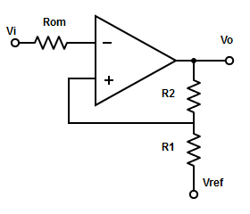
5. In which configuration a dead band condition occurs in schmitt trigger
a) Differential amplifier with positive feedback
b) Voltage follower with positive feedback
c) Comparator with positive feedback
d) None of the mentioned
View Answer
Explanation: The comparator with positive feedback is said to exhibit hysteresis, a dead band condition, when the input of comparator exceeds upper threshold voltage. At this condition, output switch from +Vsat to -Vsat. It reverts back to its original state, +Vsat when the input goes below lower threshold voltage.
6. Calculate the hysteresis voltage for the schmitt trigger from the given specification:
R2 =56kΩ , R1 = 100Ω ,Vref = 0v & Vsat = ±14v.
a) 0 mv
b) 25 mv
c) 50 mv
d) -25 mv
View Answer
Explanation: Upper threshold voltage, VUT =[R1/(R1+R2)]×( +Vsat) = [100kΩ/(56kΩ +100 Ω)]×(+14v)= +25mv.
Lower threshold voltage VLT = [R1/(R1+ R2)]×(-Vsat) = [100kΩ /(56kΩ+100Ω)]×(-14v)= -25 mv.
∴ Hysteresis voltage = VUT-VLT = 25-(-25) = 50mv.
7. How to limit the output voltage swing only to positive direction?
a) Combination of two zener diodes
b) Combination of zener and rectifier diode
c) All of the mentioned
d) Combination of two rectifier diodes
View Answer
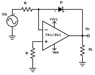
Explanation: To limit the output voltage swing to positive or negative direction, the basic op-amp comparator should be connected with a combination of zener and rectifier diode in the feedback path.
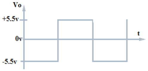
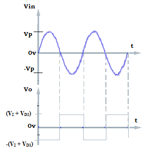
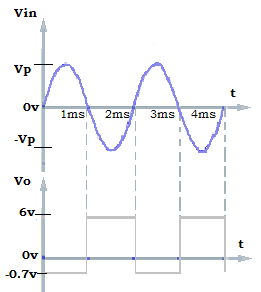
8. For the circuit shown below, obtain output waveform. Assume zener voltage to be 4.78v and voltage drop across the forward biased zener to be 0.7v.
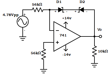
a)
b)
c)
d)
View Answer
Explanation: During positive half cycle of the input waveform, the output voltage is equal to (VZ +VD1) (because diode D1 would be in forward bias) ,
∴ (VZ +VD1) = 4.78 v+0.7 v = 5.5 v.
Similarly, during negative half cycle of the input wave form, the output voltage is equal to – (VZ +VD2) as the diode D2 would be in forward bias) , – (VZ +VD2) =- 4.78 v-0.7 v = -5.5 v.
9. A basic op-amp circuit has a zener and rectifier diode connected in the feedback path. Calculate the maximum positive voltage. Where, zener voltage = 5.1 v and voltage drop across the forward biased zener = 0.7v?
a) VO = 5.8v
b) VO = 9.9v
c) VO = 4.7v
d) VO = 7.1v
View Answer
Explanation: Initially, rectifier diode will be reverse biased and makes the op-amp to operate in open loop configuration. So, the output voltage is obtained till the rectifier diode is forward bias and zener goes into avalanche condition. Hence, the maximum positive output voltage VOz +VD (VD –> voltage drop across rectifier diode).
=> VO= 5.1v+0.7 v= 5.8v.
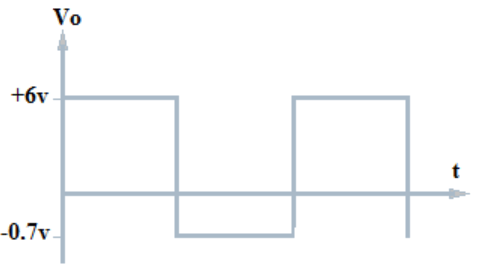
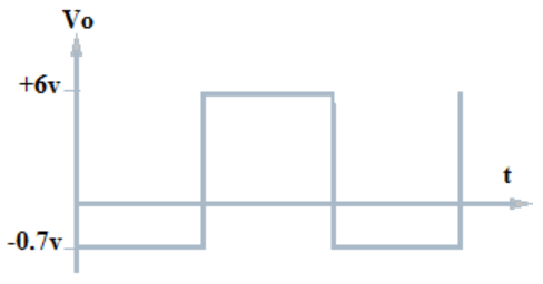
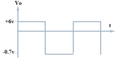
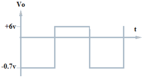
10. Use the specification and obtain the output voltage swing for op-amp comparator.
Specification: R= 1kΩ; RL=10kΩ; VZ=6v; VSat=±15v (Assume forward bias of zener = 0.7v).
a)
b)
c)
d)
View Answer
Explanation: During the positive half cycle, the output voltage would be at -VD = -0.7v because the zener will be forward biased. However, during negative half cycle of VO would be at +VZ =+6v. Thus, the zener diode in the feedback path limits VO to swing between +6v to -0.7v.
Sanfoundry Global Education & Learning Series – Linear Integrated Circuits.
To practice all areas of Linear Integrated Circuits, here is complete set of 1000+ Multiple Choice Questions and Answers.
If you find a mistake in question / option / answer, kindly take a screenshot and email to [email protected]
