This set of Linear Integrated Circuit MCQs focuses on “Active and Passive Components of IC – 3”.
1. Find the epitaxial resistor from the given cross-sectional view diagram?
a) 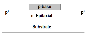
b) 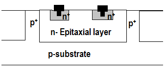
c) 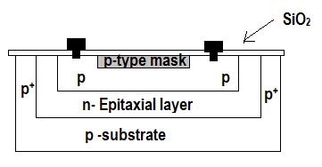
d) 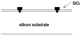
View Answer
Explanation: The mention figure is the cross sectional view of epitaxial resistor. The remaining diagrams are the cross-sectional view of pinched, thin film and diffused resistor.
2. Which integrated resistor can achieve high value of sheet resistance?
a) Pinched resistor
b) Epitaxial resistor
c) Thin film resistor
d) All of the mentioned
View Answer
Explanation: In a pinched resistor, the sheet resistivity can be increased by reducing its effective area. This technique is used to achieve high value of sheet resistance from ordinary diffused resistor.
3. How pinched resistor can give resistance in order of mega-ohm in a reasonably small area?
a) By increasing fabrication steps
b) By offering bulk resistance in n-region
c) By reducing conduction path
d) By limiting the thickness of are
View Answer
Explanation: In pinched resistor structure, one of the diode conducts in reverse direction and only a small reverse saturation current can flow through n-type material. By doing so, the effective cross-sectional area of the conduction path will be reduced and resistance between two contact lead increases.
4. Which of the following is not used as metallic film in the thin film resistor?
a) Nichrome (NiCr)
b) Tantalum (Ta)
c) Stannic oxide (SnO2)
d) Silicon dioxide (SiO2)
View Answer
Explanation: Silicon dioxide is the non-metallic layer on which the metallic thin films are deposited.
5. Pick out the incorrect statement
a) Sheet resistance have smaller and lesser parasitic components
b) Value of resistor can be easily adjusted after fabrication
c) Resistance in the range 100kΩ possible using nichrome resistors
d) Thin film resistors are more stable
View Answer
Explanation: Typically, sheet resistance value of nichrome is 40 – 400Ω/square (depending upon film thickness). So, the resistance in the range 20 to 50kΩ can only be obtained.
6. Find the equivalent circuit of junction capacitor?
a) 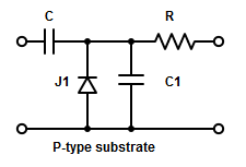
b) 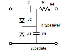
c) 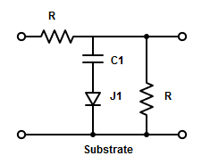
d) 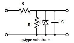
View Answer
Explanation: The mentioned diagram is the equivalent circuit diagram of junction capacitor.
7. The capacitance of junction capacitor does not depend upon
a) Impurity concentration of p-type epitaxial layer
b) Impurity concentration of n-type epitaxial layer
c) Area of the junction
d) Voltage across the junction
View Answer
Explanation: There is no p-type epitaxial layer present in junction capacitor. But a p-type substrate is present and it forms one of the junctions in the junction type IC capacitor.
8. Which is used as the dielectric layer in MOS Capacitor?
a) Silicon Nitride (Si3N4)
b) Aluminium oxide (Al2O3)
c) Tantalum oxide (Ta2O5)
d) All of the mentioned
View Answer
Explanation: Si3N4 offers higher value of capacitance. Whereas , Al2O3 and Ta2O5 are preferred for large value of capacitance. Hence all of them are used as dielectric layer.
9. Which is considered to be a serious disadvantages of thin film capacitor, when Al2O3is used as dielectric.
a) Additional fabrication step required
b) It require over voltage protection
c) Higher dielectric constant value is required
d) All of the mentioned
View Answer
Explanation: One of the serious disadvantages of thin film capacitor is that it fails, when the voltage rating exceeds due to breakdown of the dielectric, which is a destructive and irreversible failure mechanism and it require over voltage protection.
10. In MOS capacitor, the preference in dielectric layer is given to Silicon Nitride (Si3N4) because
a) It makes capacitor non-polar
b) It contain a small resistance
c) It offers less processing step
d) It reduces failure mechanism
View Answer
Explanation: Si3N4 gives more circuit flexibility by being non-polar, that is , it does not matter which plate is positive or negative and the voltage applied.
11. Why inductor is avoided in Integrated Circuit component?
a) They provide many losses compared to other IC components
b) IC devices are essentially two dimensions
c) Device density of IC increases
d) Fabrication process of these components are complicated
View Answer
Explanation: Usually, IC devices are very small (~1 to 10µm). Even if IC inductor is made in form of a flat metallic thin film spirals. Very small value of the order nanohenry with low quality factor can only be obtained.
12. Which circuit is used to replace inductor in IC components?
a) RC active network
b) PN-junction diode
c) LC active network
d) None of the mentioned
View Answer
Explanation: Circuit designer go to great lengths to avoid the use of inductors or otherwise simulate them by using RC active networks.
13. In application such as RF and IF circuits, inductor cannot be avoided. How to manage such situation?
a) Using inductors external to IC package
b) Thin film inductor spiral are used
c) Thin film hybrid microwave can be used
d) All of the mentioned
View Answer
Explanation: In most cases, inductors external to IC packages are used. However, thin film hybrid Microwave IC (MIC) and thin film inductor spiral can provide inductance up to 250nH.
Sanfoundry Global Education & Learning Series – Linear Integrated Circuits.
To practice MCQs on all areas of Linear Integrated Circuit, here is complete set of 1000+ Multiple Choice Questions and Answers.
If you find a mistake in question / option / answer, kindly take a screenshot and email to [email protected]
- Check Electrical Engineering Books
- Check Linear Integrated Circuits Books
- Apply for Electrical Engineering Internship
- Practice Electronics & Communication Engineering MCQs
- Practice Electrical Engineering MCQs
