This set of Analog Circuits Multiple Choice Questions & Answers (MCQs) focuses on “Transistor Switching Network”.
1. At saturation, which of these is not true for a BJT?
a) The collector current IC cannot increase further
b) The base current IB, cannot increase further
c) The collector-to-emitter voltage, VCE is due to the non-zero internal resistance of BJT
d) VCE(saturation) is the minimum voltage drop between C and E
View Answer
Explanation: At saturation, the collector-to-emitter voltage is the minimum drop possible occurring due to the non-zero internal resistance of the BJT. Since it cannot decrease further, the current IC cannot increase further. The BJT is said to be saturated. However, the base current, IB, can keep increasing with the input voltage and hence, in saturation, the relation IC = βIB is not satisfied.
2. For a transistor in saturation, which is true?
a) IC = βIB
b) IC > βIB
c) IC < βIB
d) IC = (β+1)IB
View Answer
Explanation: At saturation, collector current remains constant. However, the base current increases with the input voltage being applied and hence BJT cannot satisfy the relation IC = βIB. In the saturation region, βIB > IC is the correct relation.
3. Given that the BJT is completely saturated, what is the overdrive?
a) Overdrive = 1
b) Overdrive < 1
c) Overdrive > 1
d) Overdrive > 0
View Answer
Explanation: Overdrive during BJT saturation is the ratio of its normal β and its forced β. Forced β is the ratio of IC(sat) and IB when BJT is in saturation. Since in saturation IC is constant and IB increases thus, IC/IB decreases and the forced β is less than the normal β. Hence the overdrive > 1. In hard/strong saturation, β>>1.
4. Consider the graph of IC vs VI shown below for a transistor. Find the correct relation for region 3 in the diagram.
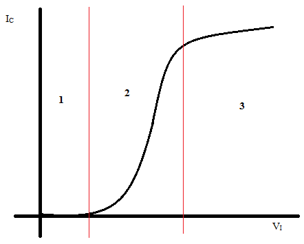
a) IC = IC(sat) and VCE = VCE(sat)
b) IC = IC(sat) and VCE = VCC
c) IC = βIB and VCE = VCE(sat)
d) IC = βIB and VCE = VCC
View Answer
Explanation: Region 3 in the above is the saturation region in which IC remains constant with respect to the input voltage and the voltage VCE is the saturation voltage, almost zero. At this point, the transistor acts as an ON switch.
5. What is the ON resistance of a transistor?
a) RON = VCEsat/βIB
b) RON = VCEsat + VA/ICsat
c) RON = VCEsat/(β+1)IB
d) RON = VCEsat/ICsat
View Answer
Explanation: In the saturation region, we consider that the transistor acts as an ON switch. In this region, both collector-to-emitter voltage as well current are constant and do not change. The ON resistance is the ratio of this saturation voltage to saturation current.
6. For the graph which depicts collector current, find the ON time.
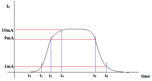
t1 = 1ms
t2 = 2ms
t3 = 4ms
t4 = 6ms
t5 = 16ms
t6 = 18ms
a) 3ms
b) 1ms
c) 2ms
d) 5ms
View Answer
Explanation: On time is the time taken by BJT to change from the OFF state to the ON state. It is the sum of the delay time and the rise time. Rise time is the time taken by current to increase from 10% to 90% of saturation and delay time is time taken by current to increase from 0 to 10% of the saturation.
ton = td + tr = t2 – t1 + t3 – t2 = 2 – 1 + 4 – 2 = 3ms.
7. Find the storage time for the current variation shown below.
t1 = 2ms
t2 = 3ms
t3 = 4ms
t4 = 6ms
t5 = 19ms
t6 = 20ms
a) 1ms
b) 13ms
c) 3ms
d) 2ms
View Answer
Explanation: Storage time is the time taken by IC to decrease from ICsat to 90% of ICsat.
TS = t5 – t4 = 19 – 6 = 13ms.
8. Which of these relations is true always for the BJT as a switch?
a) Off time >> On time
b) Off time = Storage time – Rise time
c) Off time << On time
d) Off time = Storage time + Delay time
View Answer
Explanation: Off time for a BJT is larger than its ON time. Off time=Storage time + Fall time.
Often Storage time is larger than fall/delay/rise time and hence OFF time is quite large than ON time.
9. How is BJT used as a faster switch?
a) By operating it in the saturation and cut-off region
b) By operating it in the active and cut-off region
c) By using it in strong saturation
d) By decreasing its ON resistance
View Answer
Explanation: If BJT is to act as a switch with negligible power dissipation, then BJT is operated in the cut-off and saturation region, as in the TTL family. When BJT has to be operated as a fast switch, then it is operated in the active and cut-off region, as in the ECL family.
Sanfoundry Global Education & Learning Series – Analog Circuits.
To practice all areas of Analog Circuits, here is complete set of 1000+ Multiple Choice Questions and Answers.
If you find a mistake in question / option / answer, kindly take a screenshot and email to [email protected]
