This set of Analog Circuits Questions and Answers for Entrance exams focuses on “MOSFET Amplifier with CD Configuration – 2”.
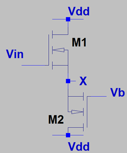
1. If g is the transconductance, r is the resistance due to channel length modulation and if M2 has channel length modulation but M1 doesn’t, what is the voltage gain at node x?
a) (1/g || r) / (1/g + (1/g || r))
b) (1/g || r) / (1/g + (1/g || 2r))
c) (1/g || r) / (2/g + (1/g || r))
d) (1/g || r) / (1/g + (2/g || r))
View Answer
Explanation: The voltage gai at node x will be due to the follower stage. Since M2 has channel length modulation, we observe that the total resistance at the source of M2 is (1/g || r). Thus, from the expression of voltage gain of a follower- the voltage gain at node x is (1/g || r) / (1/g + (1/g || r)).
2. If g is the transconductance, r is the resistance due to channel length modulation and if M2 has channel length modulation but M1 and M3 doesn’t, what is the total resistance at the source of M2?
a) (1/ g || R) || (1/g || r)
b) (1/ g) || (1/g || r)
c) R || (1/g || r)
d) (1/ g || R) || 1/g
View Answer
Explanation: The source of M2 is connected to the source of M1. Since channel length modulation isn’t present in M1, the source of M1 offers a resistance of 1/g. Again, we find the source of M2 offers a resistance of (1/g || r) due to channel length modulation. Therefore, we conclude that the total impedance at the source of M2 is (1/ g || R) || (1/g || r).
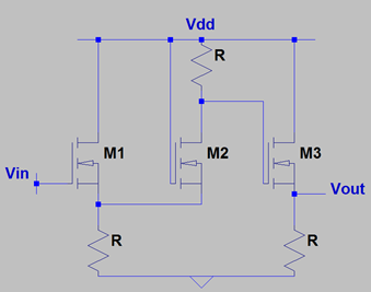
3. If g is the transconductance, r is the resistance due to channel length modulation and if M2 and M1 has channel length modulation but M3 doesn’t, what is the output resistance at the source of M3?
a) 1/g || R
b) 1/g || r + 1/g
c) 1/g || R + 1/g
d) 1/g || r + 2/g
View Answer
Explanation: The output impedance of the final stage doesn’t get affected by the previous stages since the MOSFET offers infinite impedance at the Gate. Hence, it isolates each stage from the next stage- provided the input is applied to the gate. The output impedance is simply (1/g || R) since 1/g is the impedance looking into the source of M3 while R is connected in parallel to it.
4. If g is the transconductance, r is the resistance due to channel length modulation and if M2 and M1 has channel length modulation but M3 doesn’t, what is the total resistance at the drain of M2?
a) {(1 + gr)* R + R} || 2R
b) {(1 + gr)* 3R + 2R} || R
c) {(1 + gr)* (R || 1/g || r) + (R || 1/g || r)} || R
d) Infinite
View Answer
Explanation: The drain of M2 offers a resistance of {(1 + gr)* (R || 1/g || r) + (R || 1/g || r) due to channel length modulation and the degeneration resistance R || 1/g || r connected to the drain of M2. This comes in parallel to R connected to the source of M2. Hence the overall resistance becomes {(1 + gr)* (R || 1/g || r) + (R || 1/g || r).
5. If g is the transconductance, r is the resistance due to channel length modulation and if M2 and M1 has channel length modulation but M3 doesn’t, what is the total voltage gain for only M2?
a) g * {(1 + gr)* (R || 1/g || r) + (R || 1/g || r)} || R
b) g * {(1 + gr)* R + R} || 4R
c) g * {(1 + gr)* R + 3R} || 4R
d) g * {(1 + 2gr)* R + R} || 4R
View Answer
Explanation: The voltage gain for M2 will be due to a CG stage. M2 has channel length modulation and is degenerated by (R || 1/g || r). Thus the output impedance rises to {(1 + gr)* (R || 1/g || r) + (R || 1/g || r)} ||R and hence the gain for only M2 is g * {(1 + gr)* (R || 1/g || r) + (R || 1/g || r)} || R.
6. If g is the transconductance, r is the resistance due to channel length modulation and if only M3 and M2 has channel length modulation, what is the total voltage gain?
a) R/ g * {(1 + gr)* R + R} || R * R / {(1/g || r) + R
b) R/ (1/g) * g * {(1 + gr)* R + R} || R * {(1/g || r) + R
c) R/ (1/g + R) * g * {(1 + gr)* R + R} || R * R / {(1/g || r) + 3R
d) {(R || 1/g || r) / (1/g + (R || 1/g || r)} * g * [{(1 + gr)* (R || 1/g || r) + (R || 1/g || r)} ||R] * R / {(1/g || r) + R
View Answer
Explanation: This is a cascade of a follower stage preceding a CG stage which is followed by another CD stage. The voltage gain due to first stage is {(R || 1/g || r) / (1/g + (R || 1/g || r)} since the source of M1 is connected to the source of M2 which offers a resistance of (1/g || r). The voltage gain of the next stage is due to the CG stage degenerated by (R || 1/g || r)} and the gain is g * [{(1 + gr)* (R || 1/g || r) + (R || 1/g || r)} || R]. Finally, the last stage offers a voltage gain of R / {(1/g || r) + R. After multiplying all these gains, we have the overall voltage gain as {(R || 1/g || r) / (1/g + (R || 1/g ||r)} * [g * {(1 + gr)* (R || 1/g || r) + (R || 1/g || r)} ||R] * R / {(1/g || r) + R.
7. Can the voltage gain of a follower stage be greater than 1?
a) Yes, by changing the transconductance
b) No
c) Yes, by changing the bias current
d) Yes, by changing the supply rail
View Answer
Explanation: The voltage gain of the follower stage readily tells us that it can never be used as an amplifier. It can only be used as a buffer.
8. Can the voltage gain of a follower stage be equal to 1?
a) Yes, by increasing the transconductance
b) No
c) Yes, by modifying the bias voltage
d) Yes, by modifying the bias current
View Answer
Explanation: From the expression of voltage gain, we find that if the voltage gain is 1, the transconductance has to be infinite which is practically impossible. However, we can reach a voltage gain of approximately equal to 1 but never equal to 1.
9. The output impedance of follower is less than that of a degenerated CS stage.
a) True
b) False
View Answer
Explanation: The output impedance of a CS stage will increase highly due to degeneration. Hence, it’ll be always more than that of a follower.
10. The input impedance of the follower stage is ____________ than that of a CG stage.
a) greater
b) lesser
c) equal
d) cannot be compared
View Answer
Explanation: The input to a follower stage is at the gate of the MOSFET while for a CG stage, it’s at the source of the MOSFET. Hence, the input impedance of a follower will be very much greater than that of a CG stage.
Sanfoundry Global Education & Learning Series – Analog Circuits.
To practice all areas of Analog Circuits for Entrance exams, here is complete set of 1000+ Multiple Choice Questions and Answers.
If you find a mistake in question / option / answer, kindly take a screenshot and email to [email protected]
