This set of Analog Circuits Interview Questions and Answers focuses on “Voltage-Ampere Characteristics of Diode – 2”.
1. Which of the following graph represents the I-V characteristics of a real diode?
a) 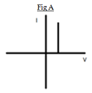
b) 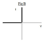
c) 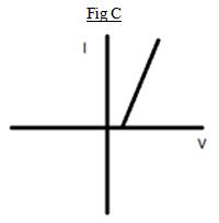
d) 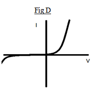
View Answer
Explanation: Fig A represents constant voltage drop model of a diode. In this model, the diode is assumed to be a perfect insulator in reverse bias. On forward bias up to the cut-in voltage, it is assumed to be an insulator and after it becomes perfect conductor. Fig B represents an ideal diode, which is in forward bias, it is a perfect conductor and in reverse bias, it is perfect insulator. We can also depict the piecewise linear mode of diode through Fig C. This assumption is very close to constant voltage drop model except the fact that after cut-in voltage instead of perfect insulator diode is assumed as a ohmic device. Fig D represents real diode. The diode in real life is similar to the characteristics. That is, after the cut-in voltage, graph is exponential and in reverse bias mode current is in micro or nano ampere range.
2. Which of the following I-V characteristics represents a typical Si diode?
a) 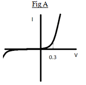
b) 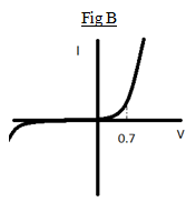
c) 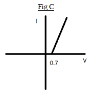
d) 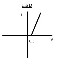
View Answer
Explanation: Fig B denotes a Si diode because the cut-in voltage is 0.7V and after this the current is exponential. Also in reverse bias there is a nano ampere range current it must also be accounted. The cut-off of 0.3V is correct for Germanium and not for a Si diode. Also, fig A, fig C & fig D which are seemingly linear are the piecewise linear model, not a real representation for the diode. Therefore, fig B is the best.
3. Which of the following graph represents a typical Ge diode?
a)
b)
c)
d)
View Answer
Explanation: Fig A denotes a Germanium diode because the cut-in voltage is 0.3V and after this the current is exponential. Also in reverse bias there is a nano ampere range current it must also be accounted. The cut-off of 0.7V is correct for Silicon and not for a Germanium diode. Also, fig B, fig C & fig D which are seemingly linear are the piecewise linear model, not a real representation for the diode.
4. Which of the following graph represent a zener diode which is voltage rated as “VZ”?
a) 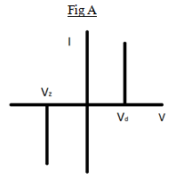
b) 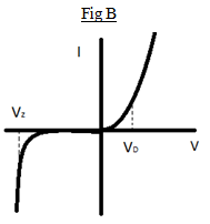
c) 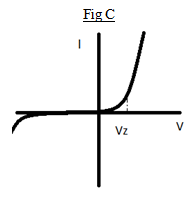
d) 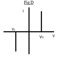
View Answer
Explanation: Voltage rating is the voltage at which reverse breakdown occurs. Voltage rating of a zener diode indicates the voltage beyond which current increases rapidly. Beyond this point increase in reverse bias voltage will only reflect on current which means voltage drop beyond this point is almost constant. At forward bias zener diode behaves as a normal diode. So the appropriate graph is fig B.
5. Which of the following statement is false for a zener diode voltage rated as “VZ“?
a) Reverse breakdown occurs at VZ
b) Forward breakdown occurs at VZ
c) Zener diode is a heavily doped diode
d) Usually operates in reverse bias mode
View Answer
Explanation: Voltage rating is the voltage at which reverse breakdown occurs. Voltage rating of a zener diode indicates the voltage beyond which current increases rapidly. Beyond this point increase in reverse bias voltage will only reflect on current which means voltage drop beyond this point is almost constant. This phenomenon holds the key role in the working of zener diode as a voltage regulator. Zener diode is a heavily doped diode because for zener breakdown we need a narrow junction. It operates in reverse bias mode. In forward bias mode it operates as a normal diode.
6. Voltage rating of a Zener diode denotes ____________
a) Reverse breakdown voltage
b) Forward breakdown voltage
c) Voltage at which current is maximum
d) Maximum forward voltage which a diode can withstand
View Answer
Explanation: Voltage rating of a zener diode indicates the voltage beyond which current increases rapidly. Beyond this point increase in reverse bias voltage will only reflect on current which means voltage drop beyond this point is almost constant. This phenomenon holds the key role in the working of zener diode as a voltage regulator.
7. Knee current in the case of zener diode implies _____________
a) Forward bias current beyond which I-V characteristics is a straight line
b) Reverse bias current above which I-V characteristics is a straight line
c) Forward cut-in current beyond which current is directly proportional to voltage
d) Maximum allowable reverse bias current through a zener diode
View Answer
Explanation: Knee current indicates the current above which reverse characteristics is a straight line. That is the relationship between current and voltage beyond this point will be directly proportional and this is very useful for solving real life problems.
8. Which of the following graph represents I-V characteristics of an ideal diode?
a)
b)
c)
d)
View Answer
Explanation: Fig A represents constant voltage drop model of a diode. In this model, the diode is assumed to be a perfect insulator in reverse bias. On forward bias up to the cut-in voltage, it is assumed to be an insulator and after it becomes perfect conductor. Fig B represents an ideal diode, which is in forward bias, it is a perfect conductor and in reverse bias, it is perfect insulator. We can also depict the piecewise linear mode of diode through Fig C. This assumption is very close to constant voltage drop model except the fact that after cut-in voltage instead of perfect insulator diode is assumed as a ohmic device. Fig D represents real diode. The diode in real life is similar to the characteristics. That is, after the cut-in voltage, graph is exponential and in reverse bias mode current is in micro or nano ampere range.
9. Which of the following I-V characteristics represents the constant voltage drop model of diode?
a)
b)
c)
d)
View Answer
Explanation: Fig A represents constant voltage drop model of a diode. In this model, the diode is assumed to be a perfect insulator in reverse bias. On forward bias up to the cut-in voltage, it is assumed to be an insulator and after it becomes perfect conductor. Fig B represents an ideal diode, which is in forward bias, it is a perfect conductor and in reverse bias, it is perfect insulator. We can also depict the piecewise linear mode of diode through Fig C. This assumption is very close to constant voltage drop model except the fact that after cut-in voltage instead of perfect insulator diode is assumed as a ohmic device. Fig D represents real diode. The diode in real life is similar to the characteristics. That is, after the cut-in voltage, graph is exponential and in reverse bias mode current is in micro or nano ampere range.
10. Which of the following statement about a Si diode is true?
a) Cut-in voltage is always higher than the reverse breakdown voltage
b) Reverse saturation current is in the order of mA
c) Cut-in voltage is 1V
d) Reverse scale current is in the order of nA
View Answer
Explanation: Cut-in voltage of Si diode is 0.7V but reverse breakdown voltage is almost 50V for the Si diode. So clearly cut-in voltage is much less than the reverse breakdown voltage. Reverse saturation current is in the order of nano amperes. Scale current is another name of saturation current. It is named as scale current because saturation current is directly proportional to cross sectional area of a diode.
Sanfoundry Global Education & Learning Series – Analog Circuits.
To practice all areas of Analog Circuits for Interviews, here is complete set of 1000+ Multiple Choice Questions and Answers.
If you find a mistake in question / option / answer, kindly take a screenshot and email to [email protected]
