This set of Analog Circuits Questions and Answers for Aptitude test focuses on “MOSFET Amplifier with CS Configuration – 2”.
1. What is the input impedance of the following C.S. stage?
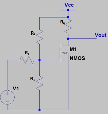
a) R2 || R3
b) R1 || (R2 + R3)
c) (R1 || R2) + R3
d) R1 + (R2 || R3)
View Answer
Explanation: The input impedance can be calculated by performing a small signal analysis at the input side ie the Gate of M1. We need to set Vcc and V1 to 0 and place a voltage source at the node after R1. Henceforth we find that R2 and R3 are simply connected from the same node to ground so they are parallel to each other. Note that by input impedance of the C.S. stage, we refer to the impedance seen by the signal after it crosses R1.
2. Neglecting Channel Length Modulation, what is the output impedance of the following C.S. stage?
a) R4
b) R4 || R2
c) R4 || (R2 + R3)
d) R4 || [(R2 + R3) || R1]
View Answer
Explanation: The output impedance is calculated by a simple small signal analysis. We set Vcc and V1 to 0 and place a voltage source at the output node. We find that only R4 is the output impedance. Note that even if R2 seems to be connected to R4, it doesn’t affect the output impedance since during small signal analysis, the node where R2 and R4 meets, is set to ground.
3. In the following C.S. stage, what is the gate voltage appearing across M1?
a) V1 * [(R2 || R3) / (R1 || R2 || R3)]
b) V1 * [(R2 + R3) / {R1 + R2) || R3}]
c) V1 * [(R2 + R3) / (R1 + R2 + R3)]
d) V1 * [(R2 || R3) / {R1 + (R2 ||R3}]
View Answer
Explanation: The Thevenin resistance seen by the input voltage V1 is R1 + (R2 || R3). The Thevenin resistance is calculated by setting Vcc to 0 and hence calculating the current entering the C.S. stage. After finding the Thevenin Resistance, it is found that the voltage drop across the gate of M1 is due to a potential divider between R1 and (R2 || R3) where the voltage across (R2 || R3) is truly the gate voltage. Hence, the total gate voltage V1 is attenuated and becomes V1 * [(R2 || R3) / {R1 + (R2 ||R3}] .
4. If an NMOS is degenerated by a resistor in series with the source, what will happen to the output resistance?
a) It increases
b) It decreases
c) It remains same
d) Cannot be determined
View Answer
Explanation: This is a fact derived by performing the small signal analysis of a degenerated C.S. stage. The output impedance increases if we degenerate the MOSFET and this further increases the linearity of operation.
5. If we have 3 resistors of 1k, 2k and 3k, how should they be used amongst R1, R2 and R3 to get the maximum gate voltage in the following C.S. stage?
a) R1 = 1k, R2 = 2k, R3 = 3k
b) R1 = 3k, R2 = 2k, R3 = 1k
c) R1 = 2k, R2 = 1k, R3 = 3k
d) R1 = 3k, R2 = 1k, R3 = 2k
View Answer
Explanation: The Thevenin resistance seen by V1 is R1 + (R2 || R3). The gate voltage is a result of V1 going through a potential divider of R1 and (R2 || R3) where the voltage across (R2 || R3) is essentially the gate voltage ie V1 * [(R2 || R3) / { R1 || R2 || R3) }]. Hence, we need to maximize (R2 || R3) which is possible if R2=2k and R3=3k. This implies R1 has to be equal to 1k.
6. If Vth is .45V, what is the output voltage for the following C.S. stage?
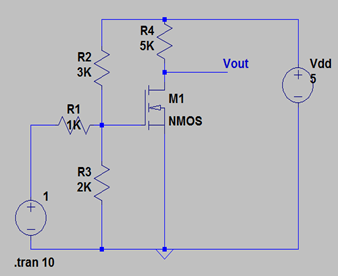
a) 4.7 V
b) 3.9 V
c) 2.1 V
d) 3.5 V
View Answer
Explanation: Firstly, we know that the voltage gain from the gate to the source is gm * R4. We observe that Vg is Vin * [(R2 || R3) / {R1 || R2 || R3}, where Vin is 1v and the values of R1, R2 and R3 are provided, which is roughly equal to .55V. This .55V is getting amplified by a factor of gm*R4. Now, Vout is related to Id, the drain current, as Vdd – Id*R4. Again, we know that gm = 2Id/Vgs-Vth. So, we have 2 equations as follows:
i. Vout = gm*R4 = 2*Id/(Vgs – Vth)*R4
ii. Vout = Vdd – Id * R4
We have the values of all the parameters. Solving for Vout will yield Vout as 4.7V.
7. What is the output voltage in the following C.S. stage?
a) 5 V
b) 0 V
c) 2.5 V
d) 3 V
View Answer
Explanation: There is no resistor placed between the drain and the supply voltage, Vdd. Hence, Vout is nothing but 5V.
8. What is the role of the capacitor in the following circuit?
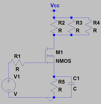
a) Increasing the gain
b) Decreasing the gain
c) Has not role
d) Decreases the output impedance
View Answer
Explanation: We note that this circuit is an example of a degenerated C.S. stage. If the impedance connected at the source terminal is very low, the voltage gain of the circuit increases. The capacitor is called a bypass capacitor as it helps to provide a path of much less resistance than R5. The magnitude of capacitance can be controlled, to an extent, according to the frequency of operation.
9. Coupling capacitors provide D.C. coupling during biasing of transistors.
a) True
b) False
View Answer
Explanation: Capacitors always block D.C. signals. In fact, they provide A.C. coupling to ensure that the biasing of consecutive stages of transistors do not get affected by the individual biased conditions.
10. If \(\frac{1}{2}\)µnCox*(W/L) = K and λ=0 for the C.S. stage shown below, what is the voltage gain (ideally)?
a) (R2 || R3 || R4) * 3K * (V1 – 2Vth)
b) (R2 || R3 || R4) * K * (V1 + Vth)
c) (R2 || R3 || R4) * 2K * (V1 – Vth)
d) (R2 || R3 || R4) * K * (V1 – Vth)
View Answer
Explanation: Ideally, the bypass capacitor would short the source terminal of the M1 to ground. Hence, this becomes a simple C.S. stage instead of a degenerated C.S. stage. Hence, the gain is simply gm*(total resistance connected at the drain). The total resistance connected at the drain is (R2 || R3 || R4) since all the three resistors are parallel to each other. The transconductance(gm) is K(V1-Vth). Hence the overall voltage gain is (R2 || R3 || R4) * K * (V1 – Vth).
Sanfoundry Global Education & Learning Series – Analog Circuits.
To practice all areas of Analog Circuits for Aptitude test, here is complete set of 1000+ Multiple Choice Questions and Answers.
If you find a mistake in question / option / answer, kindly take a screenshot and email to [email protected]
