This set of Analog Circuits Multiple Choice Questions & Answers (MCQs) focuses on “Diode Basics and Equivalent Circuits”.
1. Which of the following is not a valid form of a diode equivalent circuit?
a) Piecewise Linear Model
b) Ideal Diode Model
c) Simplified Model
d) Differential Model
View Answer
Explanation: Differential model doesn’t define any diode. It defines an Operational Amplifier.
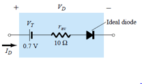
2. Which model of the diode equivalent circuit is represented by the given diagram?
a) Piecewise Linear Model
b) Ideal Diode Model
c) Simplified Model
d) Differential Model
View Answer
Explanation: This model involves a voltage drop and a resistance in series with an ideal diode and hence it represents the Piecewise Linear Model.
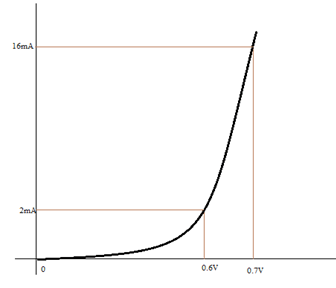
3. From the given I-V characteristics of a silicon diode, what is the approximate value of rav between marked points?
a) 7 ohms
b) 11.2 ohms
c) 8 ohms
d) 6 ohms
View Answer
Explanation: rav is the average AC resistance, found between two marked points in the I-V graph. Here rav=0.1/14mA=7Ω.
4. AC resistance of a diode was found to be r1 and r2, when measured with two different values of diode current i.e. 10 mA and 25 mA respectively, for the same diode voltage. Which of the following options hold true?
a) r1 = r2
b) r1 > r2
c) r1 < r2
d) Can’t be determined
View Answer
Explanation: r1 > r2 as AC resistance is inversely proportional to the diode current.
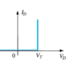
5. Which of the following models of diode equivalent circuit is represented by the given I-V characteristic curve?
a) Piecewise Linear Model
b) Ideal Diode Model
c) Simplified Model
d) Hybrid model
View Answer
Explanation: In simplified model, the value of rd is neglected and hence, we get a high value of current for voltage greater than or equal to VT.
6. What is the approximate value of voltage across the silicon diode for the diagram given?
a) +0.7 V
b) 0 V
c) +10 V
d) -10 V
View Answer
Explanation: -10 V. The operating characteristic of a diode operating in the reverse bias region suggests that beyond a certain threshold current, the voltage across the diode is nearly constant = reverse breakdown voltage.
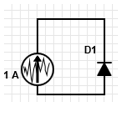
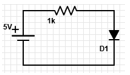
7. Assuming the diode in the given circuit diagram to be a silicon p-n junction diode, what is the current for the given circuit diagram?
a) 4.3 mA
b) 0
c) 43 mA
d) 5 mA
View Answer
Explanation: The diode in the circuit is reverse biased and hence the current is zero.
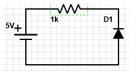
8. Assuming the diode in the given circuit diagram to be a silicon p-n junction diode, what is the current for the given circuit diagram?
a) 0
b) 5 mA
c) 4.3 mA
d) Can’t be determined
View Answer
Explanation: 4.3 mA. The silicon diode in the circuit is forward biased. Considering a voltage drop of 0.7 V across the diode, the voltage drop across the resistor is (5-0.7) V = 4.3 V. Hence, Current in the circuit = Current through the resistor = (4.3/1000) A = 4.3 mA.
9. The reverse saturation current for a Germanium diode at a temperature of 293 K is found to be 2 μA. What is the reverse saturation current Is at a temperature of 313 K?
a) 2 μA
b) 8 μA
c) 4 μA
d) Can’t be determined
View Answer
Explanation: The reverse saturation current for a silicon diode doubles its value for every 10 K rise in temperature. Hence Is at 313 K=2 x 2 x 2 = 8 uA.
10. During the reverse bias operation of a p-n junction diode, the width of the depletion region increases. Is the given statement true or false?
a) True
b) False
View Answer
Explanation: During reverse bias operation of a diode, the width of the depletion region increases leading to extremely high values of resistance and hence negligible values of current.
11. The threshold voltage of a diode at Antarctica and India were found to be V1 and V2 respectively. Which of the following relations between V1 and V2 hold good?
a) V1 > V2
b) V1 = V2
c) V1 < V2
d) Can’t be determined
View Answer
Explanation: Temperature in India is greater than that in Antarctica. Hence, the reverse saturation current measured in India will be higher as compared to that measured in Antarctica. Now, as Is and VT are inversely related, V1 >V2.
Sanfoundry Global Education & Learning Series – Analog Circuits.
To practice all areas of Analog Circuits, here is complete set of 1000+ Multiple Choice Questions and Answers.
If you find a mistake in question / option / answer, kindly take a screenshot and email to [email protected]
