This set of Analog Circuits Assessment Questions and Answers focuses on “MOSFET Amplifier with CG Configuration – 2”.
1. If the inverse of transconductance is .5KS-1, what should be the value of Rc so that the overall voltage gain is 8?
a) About 3K
b) .4K
c) About 4K
d) Such a gain is not possible
View Answer
Explanation: The voltage gain is given by gmRd. So, gm become 2mS and a resistance of 4k Ω will be necessary.
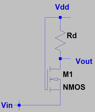
2. What is the input impedance of the following circuit, if channel length modulation is present?
a) gm || 1/ro
b) gm * ro
c) gm || 2/ro
d) gm
View Answer
Explanation: The input impedance can be found by performing a small signal analysis at the input node i.e. source of the MOSFET. Due to channel length modulation, the effect of ro would make the input impedance gm || 1/ro.
3. The C.G. stage can be regarded as a current buffer.
a) True
b) False
View Answer
Explanation: The input current flows through the source of the MOSFET while the gate current is nearly equal to 0. Hence, the entire current coming out of the drain is due to the source current.
4. If M1 suffers from channel length modulation but M2 doesn’t, what is the voltage gain?
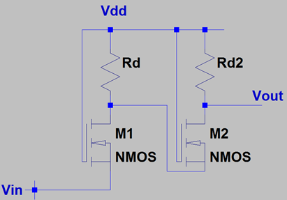
a) gm1 * Rd || 1/gm2 * gm2 * Rd2
b) gm1 * Rd || 1/gm2 * gm2 * 2Rd2
c) gm1 * Rd || 12/gm2 * gm2 * Rd2
d) gm1 * Rd * gm2 * Rd2
View Answer
Explanation: The voltage gain due to M1 is gm1 * Rd || 1/gm2 since we find that the drain of M1 is connected to the source of M2 and the impedance looking into the source of a MOSFET is 1/gm2. Now, the voltage gain due to the 2nd CG stage is simply gm2*Rd2. Hence, the total voltage gain is a product of both the factors ie gm1 * Rd || 1/gm2 * gm2 * Rd2.
5. If M2 suffers from channel length modulation but M1 doesn’t, what is the voltage gain?
a) 2gm1 * Rd || 1/gm2 * gm2 * Rd2
b) 2gm1 * Rd || 1/gm2 * gm2 * 2Rd2
c) gm1 * Rd || 12/gm2 * gm2 * Rd2
d) gm1 * Rd || 1/gm2 || ro2 * gm2 * Rd2
View Answer
Explanation: The voltage gain due to M1 is gm1 * Rd || 1/gm2 || ro2 since we find that the drain of M1 is connected to the source of M2 and the impedance looking into the source of a MOSFET is 1/gm2 || ro2 due to the channel length modulation of M2. Now, the voltage gain due to the 2nd CG stage is simply gm2*Rd2. Hence, the total voltage gain is a product of both the factors ie gm1 * Rd || 1/gm2 * gm2 * Rd2.
6. If channel length modulation is present, what is the total impedance at node X?
a) Rd || ro1 || 1/gm2
b) Rd || ro1 || 1/gm2 || ro2
c) Rd || 2ro1 || 1/gm2 || ro2
d) Rd || ro1 || 2/gm2 || ro2
View Answer
Explanation: We develop a Thevenin’s equivalent w.r.t. node X and ground. But this is lengthy process. But then again, we can use the process as follows. For Thevenising, firstly we set Vdd and Vin to ground. Thereafter, we see that Rd and ro1 are in parallel to each other since they are connected from node X to ground. Next, we see that the impedance provided by M2 is 1/gm2 || ro2 but it again occurs from Node x to ground. Hence, all the impedances are parallel to each other and the total impedance at node X is Rd || ro1 || 1/gm2 || ro2.
7. For an ideal current source, what is the voltage gain of the following circuit?
a) gm1 * rd1 * gm2 * 2Rd2
b) – gm1 * rd1 * gm2 * Rd2
c) 2gm1 * rd1 * gm2 * Rd2
d) – gm1 * rd1 * gm2 * Rd2
View Answer
Explanation: The voltage gain for the C.G. stage is simply gm * Rd1. The voltage gain of the next stage is – gm * Rd2. Note that, the ideal current source exhibits infinite output impedance and doesn’t affect but only increases the linearity of operation.
8. How can we reduce the number of MOSFET’s in the following circuit?

a) Scale the aspect ratio
b) Increase the transconductance
c) Increase the Power supply
d) Not possible
View Answer
Explanation: increasing the transconductance or power supply is possible but we need to increase our power budget for both situations which is not possible. However, we can increase the aspect ratio of one MOSFET. This is because the total current entering into R1 is a sum of the currents originating from the drain of each MOSFET and they are equal to each other. Hence, scaling the aspect ratio is a plausible situation.
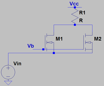
9. What is the relation between Vb and Vin in the following circuit?
a) Vb > Vin by Vth
b) Vb = Vin
c) Vb < Vin by Vth
d) No relation
View Answer
Explanation: To turn an NMOS on, we need to keep the voltage difference between the gate and the source greater than the threshold voltage. Hence, the gate potential should greater than the source potential by Vth.
10. What is the total output impedance at node x?

a) R1 || ro1 || 2 * ro2 || ro2 || 2*ro4 … || ron
b) R1 || 2 * ( ro1 || ro2 … || ron)
c) R1 || ro1 || ro2 … || ron
d) R1 + (ro1 || ro2 … || ron)
View Answer
Explanation: We note that all the MOSFET’s are in parallel. The output impedance of the ith MOSFET is given by roi. Hence, the total impedance at node x is simply R1 || ro1 || ro2…|| ron. Note that R1 is parallel to each MOSFET. This is because, while dining the output impedance, we set Vin and Vcc to zero. Note that R1 is connected from node X to ground, all the MOSFET’s are connected form node x to ground.
Sanfoundry Global Education & Learning Series – Analog Circuits.
To practice all areas of Analog Circuits Assessment Questions, here is complete set of 1000+ Multiple Choice Questions and Answers.
If you find a mistake in question / option / answer, kindly take a screenshot and email to [email protected]
