This set of Analog Circuits Multiple Choice Questions & Answers (MCQs) focuses on “JFET Amplifier”.
1. What are the small signal FET parameters?
a) gm and rds
b) gm and Vgs
c) Vds and rds
d) gm
View Answer
Explanation: The small signal model of FET- MOSFET and JFET is obtained from the following equation IDS = gmVgs + Vds/rds
gm and rds are the small signal FET parameters.
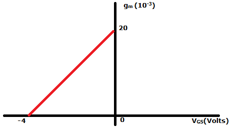
2. Find the transconductance when applied gate to source voltage is -2V.
a) 10 Ω-1
b) 10mΩ-1
c) 40mΩ-1
d) 20mΩ-1
View Answer
Explanation: VP = -4V
gm = gmo (1 – VGS/VP) = 20 (1-2/4) = 20/2 = 10mΩ-1.
3. Choose the incorrect statement for JFET(s).
a) Maximum transconductance occurs at VGS=0
b) Transconductance decreases linearly with VGS
c) Transconductance increases linearly with IDS
d) Transconductance does not depend on VDS
View Answer
Explanation: Maximum transconductance occurs at VGS = 0, and it lies between 0-gmo. Transconductance decreases linearly with VGS according to equation gm = gmo(1-VGS/VP). However, gm ∝ \(\sqrt{I_{DS}}\), which is a parabolic increase, not linear.
4. Consider the circuit shown below.
Find the net output resistance given that gm = 1mΩ-1 and rds = 0.1 MΩ.
a) 10 kΩ
b) 9.09 kΩ
c) 100 kΩ
d) 110 kΩ
View Answer
Explanation: Net output resistance for the circuit is R = rds||RD = 100k||10k
R = 9.09 kΩ.
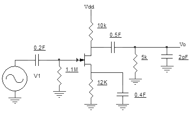
5. For an RC coupled common source JFET amplifier without bypass capacitor, find the voltage gain if gm = 1mΩ-1, source resistance is 2kΩ, drain resistance is 15kΩ and load is 10kΩ.
a) -2
b) -2.5
c) 5
d) 2
View Answer
Explanation: AV = -gmRL’/1+gmRS
RL’= 15k|| 10k = 6kΩ
AV = – 2.
6. Consider the amplifier below.
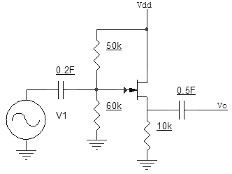
Find the input resistance and voltage gain of the circuit, given gm = 0.5mΩ-1 and rds = 0.2MΩ.
a) RI = 27.27 kΩ, AV = 5
b) RI = 44 kΩ, AV = 1
c) RI = 27.27kΩ, AV = 1
d) RI = 60kΩ, AV = 100
View Answer
Explanation: The given circuit is a common drain JFET amplifier.
Its input resistance, RI = RG = 60k||50k = 27.27 kΩ
The voltage gain is 1.
7. Which of these is incorrect for a common gate amplifier?
a) It is a current buffer
b) It has ∞ output resistance
c) Its input resistance is high
d) It is used as a high-frequency amplifier
View Answer
Explanation: A common gate amplifier can be used as a current buffer since its current gain is 1. It has very high output resistance (∞) and low input resistance. It is often used as a high-frequency amplifier.
8. In a high-frequency model of a JFET, which of these capacitances is present?
A: Gate-to-source capacitance
B: Gate-to-drain capacitance
C: Drain-to-source capacitance
a) A and B
b) A and C
c) B and C
d) A, B and C
View Answer
Explanation: In an HF model of a JFET, CGS and CGD are present, in the range of 1pF to 10 pF. CDS is the internal capacitance of the channel, ranging from 0.1pF to 1pF.
9. Which of these is false for a CS amplifier without a bypass capacitor compared to a CS amplifier with a bypass capacitor?
a) Voltage gain magnitude decreases
b) Input resistance remains same
c) The output resistance decreases
d) The output is 180° out of phase with respect to the input applied
View Answer
Explanation: For a CS amplifier without a bypass capacitor, the input resistance is unchanged and output resistance increase.
RI = RG for both.
RO = rds with bypass capacitor and rds = rds + (1+μ) RS without a bypass capacitor.
Output is still 180° out of phase compared to applied input, but the gain decreases.
10. Which of these has an output which follows input?
a) CS amplifier with a bypass capacitor
b) CD amplifier
c) CG amplifier
d) CS amplifier without a bypass capacitor
View Answer
Explanation: For a CD amplifier, the gain AV = gm(RS||rds)/1+gm(RS||rds)
But since gm(RS||rds)>>1, gain AV≈1, that is, it acts as a voltage follower. It is also called a source follower.
11. In a CS amplifier, given that rds=0.5MΩ and gm=5mΩ-1, the load is 10kΩ, source resistance is 44 kΩ. Calculate the internal amplification factor for the small signal model.
a) 2500
b) 8100
c) 9800
d) 7700
View Answer
Explanation: When the current source in small signal mode, gmVGS is converted into a voltage source, the source is equal to μVGS where μ=gmrds is the amplification factor of the circuit.
Hence, amplification factor = 2500.
Sanfoundry Global Education & Learning Series – Analog Circuits.
To practice all areas of Analog Circuits, here is complete set of 1000+ Multiple Choice Questions and Answers.
If you find a mistake in question / option / answer, kindly take a screenshot and email to [email protected]
- Practice Electrical & Electronics Engineering MCQs
- Practice Electrical Engineering MCQs
- Apply for Electrical & Electronics Engineering Internship
- Check Electrical Engineering Books
- Check Analog Electronics Books
