This set of Analog Circuits Multiple Choice Questions & Answers (MCQs) focuses on “Clamper Circuit”.
1. Which of the following is not true regarding clamper?
a) A positive clamper adds a positive DC voltage
b) A clamper can also be called as a re-inserter
c) To reduce tilt, reduce the RC value
d) Negative clamper will clamp the positive peak of output to the reference voltage
View Answer
Explanation: Clamper is called a re-inserter since it adds DC voltage to wave, inserts DC. Also, a positive clamper adds a positive DC voltage, shifting the wave up, and vice versa for the negative clamper. However, to reduce the tilt in the output, RC should be large, not small.
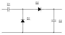
2. What is A, B, C and D to design a voltage doubler in the given circuit?
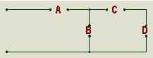
a) A=B=Resistors, C=D=Diodes
b) A=D=Capacitors, B=C=Diodes
c) A=Capacitor, B=D=Diodes, C=Resistor
d) A=C=Diodes, B=D=Capacitors
View Answer
Explanation: During the negative cycle, D1 conducts and C1 charges up to peak input. When the input is positive, then D2 conducts and C2 charges up to 2Vm. This creates a voltage doubler.
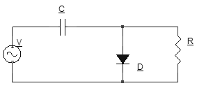
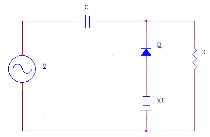
3. Consider the circuit provided. Total discharge time = 0.5 ms. Consider the diode to be an ideal diode, for a square wave input of ± 10 V, what is the percentage tilt? (C = 1MF & R = 50k Ohms)
a) 10%
b) 1%
c) 0.1%
d) 1.1%
View Answer
Explanation: Total discharge time Td=0.5ms. For ideal diode, no cut-in voltage.
% Tilt = ΔVo/2Vm * 100
Idischarge = 2Vm/R = 2*10/50k = 0.4 mA
ΔVo = Tdischarge*Idischarge/C = 0.5ms*0.4mA/1MF = 0.2
% Tilt = (0.2/20) * 100 = 1 %.
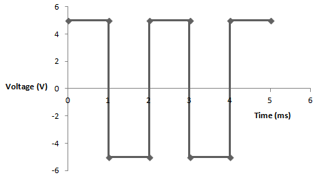
4. Given input for the circuit is f = 1 KHz.
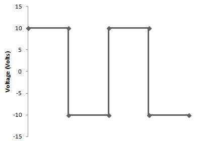
Diode cut-in voltage = 0.7 V
Output waveform:
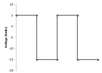
For the given output, find V1 and discharge time?
a) 4.3 V, 1ms
b) 4V, 0.5ms
c) 4.3V, 0.5ms
d) 5.7V, 1ms
View Answer
Explanation: Original wave is from +10V to -10V. The final square wave is from +5V to -15V. Negative DC voltage is added, it’s a negative clamper.
Thus, Vo = 5 V when Vin = 10 V. Vcut-in = 0.7 V
Then, Vo = Vin – (V1 + Vcut-in) = 10 – (V1 + 0.7) = 5
Therefore V1 = 4.3 V
Discharge time = To/2 ; To = 1/fo = 1/1000 = 1 ms; Discharge time = 0.5 ms.
5. In the given circuit, given that C=2MF and diode cut-in voltage, Vγ =0. Calculate the average output voltage.
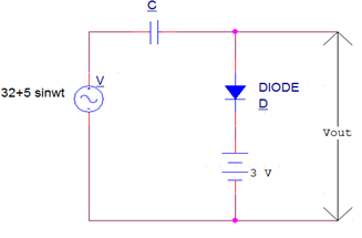
a) 2V
b) 4V
c) -2V
d) -3V
View Answer
Explanation: Maximum input is Vm = 32 + 5 = 37 V
Capacitor charges up to 37 – 3 = 34 V
Vout = Vin – Vc = 32 + 5 sinωt – 34 = -2 + 5sinωt
Average output voltage = – 2 V.
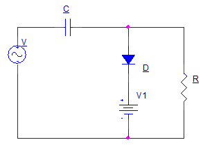
6. Considering a clamper circuit, where capacitance C, load R, the cut-in voltage of diode are unknown, which is the correct statement?
a) The DC level of the signal changes
b) The peak-to-peak value of signal changes
c) The shape of signal changes
d) The DC level shifts up
View Answer
Explanation: The shape and peak to peak value of signal remain unchanged in a clamper. A clamper only affects the DC voltage level of the wave, which can be both moved up and down, not simply up.
7. Tilt of output waveform for the circuit is 1%. Given that input is a square wave ± 10 V, f = 2 kHz, diode cut-in voltage = 0.7, what is the relation between C and R?
a) RC=20
b) RC=1/2
c) RC=2
d) RC=1/20
View Answer
Explanation: To = 1/f = 1 ms; Tdischarge = 0.5 ms
Tilt = 100 *ΔVo/2Vm = 100 *ΔVo/20 = 5 * ΔVo = 1
Thus ΔVo = 0.2 = Idischarge * Tdischarge/C
Idischarge/C = 0.2/Tdischarge = 0.2/0.5 ms = 400
RC = 2Vm/400 = 20/400 = 1/20.
8. If input diode is an ideal diode. Which output waveform across R is valid for values of V1 from +2 to + 4 volts?
a) 
b) 
c) 
d) 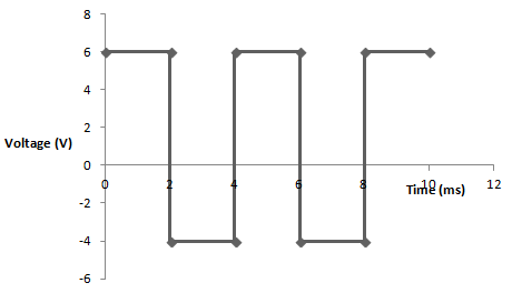
View Answer
Explanation: The waveform cannot change its frequency since a clamper only effects DC level of waveform. Also, the peak-to-peak value of wave does not change due to a clamper.
Since the bias voltage starts from 2V, the output waveform cannot start from 0V.
9. Choose the correct option for the relation between the two circuits.
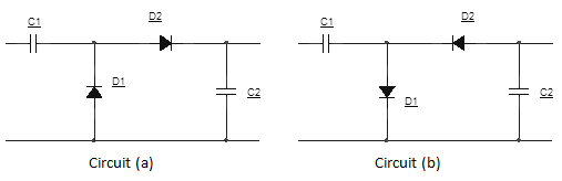
a) Circuit (a) is a voltage doubler circuit, while Circuit (b) does not double the voltage
b) Both are similar and double the voltage to 2Vm
c) Circuit (a) is a doubler circuit with output +2Vm and Circuit (b) is a doubler with output -2Vm
d) Circuit (a) is a doubler circuit, while Circuit (b) is a clipper
View Answer
Explanation: Both circuits are half-wave voltage doublers, in which capacitor C2 charges up to twice the positive (or negative for Circuit (b)) peak for one half of the wave. Neither of the circuits acts as a clipper.
10. Consider the circuit shown. The input is a square wave ± 15 V, for a silicon diode and an output voltage swing of 30 V. Choose the validity of the statement. If the value of resistance R = 10KΩ and capacitance C = 1MF.
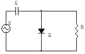
a) True
b) False
View Answer
Explanation: The output voltage swing is always equal to the input voltage swing. The output swing doesn’t depend on the values of R and C. All values are valid, RC values only are changed to decrease the tilt /distortion.
Sanfoundry Global Education & Learning Series – Analog Circuits.
To practice all areas of Analog Circuits, here is complete set of 1000+ Multiple Choice Questions and Answers.
If you find a mistake in question / option / answer, kindly take a screenshot and email to [email protected]
- Apply for Electrical Engineering Internship
- Apply for Electrical & Electronics Engineering Internship
- Practice Electrical Engineering MCQs
- Check Electrical Engineering Books
- Check Analog Electronics Books
