Analog Circuits Questions and Answers – MOSFET Amplifier with CS Configuration – 1

This set of Analog Circuits Multiple Choice Questions & Answers (MCQs) focuses on “MOSFET Amplifier with CS Configuration – 1”.

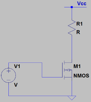
1. Neglecting Channel Length Modulation, what is the voltage gain from the gate to the drain of M1?
Find the voltage gain from the gate to the drain of M1 in given circuit
a) gm * R1
b) gm * 2R1
c) gm * R1 || RO
d) 3gm * R1
View Answer

Answer: a
Explanation: We construct the rπ model and find that the voltage gain from the gate to the drain of the MOSFET is gm * R1. Since Channel Length Modulation is neglected, the voltage gain won’t be gm * R1 || RO.

2. In the following C.S. stage shown below, what is the transconductance?
Find the transconductance in C.S. stage due to a small change in the input voltage
a) \(\frac{1}{2}\)µnCox*(W/L)(V1-Vth)
b) 3µnCox*(W/L)(V1-Vth)
c) µnCox*(W/L)(V1-Vth)
d) 2µnCox*(W/L)(V1-Vth)
View Answer

Answer: a
Explanation: The transconductance is the ratio of a small change in the output current due to a small change in the input voltage. By differentiating the equation relating the current to the input voltage of a MOSFET with respect to the input voltage, we’ll get \(\frac{1}{2}\)µnCox*(W/L)(V1-Vth).

3. In the following C.S. stage shown below, what is the input impedance (ideally) if channel length modulation is neglected?
Find the input impedance in C.S. stage in the gate of the MOSFET
a) Infinite
b) Very high
c) Very low
d) Cannot be determined
View Answer

Answer: a
Explanation: Ideally, the input impedance while looking into the gate of the MOSFET is infinite. This is because of the SiO2 layer which behaves as an insulator.
advertisement
advertisement

4. In the following C.S. stage shown below, what is the input impedance if λ>0?

5. In the following C.S. stage shown below, what is the output impedance if λ>0?

6. In the following C.S. stage shown below, what is the output impedance, if channel length modulation is neglected?
Find the output impedance in C.S. stage if output impedance is R1
a) 2ro
b) 5
c) R1
d) 0
View Answer

Answer: c
Explanation: If the early effect is neglected, ro –> ∞ and hence, the output impedance is only R1. This is inferred by performing the small signal analysis at the output node or the drain of the M1.

7. In the following C.S. stage shown below, what is the voltage gain from the gate to the drain of M1 if λ>0?

advertisement

8. If the output voltage is sensed at the collector, which of the following option perfectly describes the stage shown below?
The degenerated CS stage because current source connected at the source of M1
a) A degenerated C.S. stage
b) A C.S. stage
c) A shunted C.S. stage
d) An open C.S. stage
View Answer

Answer: a
Explanation: The above shown stage is a degenerated CS stage. This stage is called so because the current source connected at the source of M1 reduces the total gain of the CS stage. The current source provides a finite output impedance which is connected the source. Thereby, the overall gain decreases.

9. What is the overall input resistance of the CS stage shown below?
Find the overall input resistance of the CS stage if input resistance is R3
a) R3
b) R3 || R1
c) 2 * R3
d) Infinite
View Answer

Answer: a
Explanation: By performing a simple small signal analysis, we find that the input resistance is simply R3. The impedance is not infinite since we have a resistor between the gate and the input voltage.
advertisement

10. If the output impedance of the current source is Ri, what is the output impedance of the CS stage shown below, if channel length modulation is neglected?
Find the output impedance of the CS stage if output impedance of the current source is Ri
a) (1 + gm * (R1 || R2)) * Ri + (R1 || R2)
b) {R1 * (R2 + ro)} || Ri
c) R1 || R2
d) 0
View Answer

Answer: a
Explanation: We calculate the output impedance by shorting the two voltage sources to ground. Thereafter, as we apply a simple step input at the output node, i.e. the collector node, we’ll find that the total impedance at connected to the drain of M1 is nothing but (1 + gm * (R1 || R2)) * Ri + (R1 || R2) where gm is the transconductance of M1, R1 || R2 is the total resistance connected at the drain and Ri is the total resistance connected at the source. The output impedance would’ve been R1 || R2 if the current source was absent.

11. If the transconductance of M1 is 5S, voltage gain for the following degenerated CS stage is _____
Find voltage gain for the degenerated CS stage if the transconductance of M1 is 5S
a) 2.45
b) 1.25
c) 1.45
d) 2.25
View Answer

Answer: b
Explanation: The voltage gain for a degenerated CS stage is \(\frac{-Rd}{(\frac{1}{gm} + Rs)}\). Hence, after putting the values, we get 5/4 and hence the answer becomes 1.25. Rd is the total resistance connected to the drain of the M1 while Rs is the total resistance connected to the source of the M1.

12. If both the MOSFET’s are identical, what is the voltage gain from V1 to node S?
Find the voltage gain from V1 to node S for identical MOSFET’s
a) Vcc – 2R1 * µn Cox * (W/L) * (V1-Vth)2
b) Vcc R1 * \(\frac{1}{2}\)µn Cox (W/L) * (V1-Vth)2
c) Vcc – R1 * µn Cox (W/L) * (V1-Vth)2
d) Vcc – 4R1 * \(\frac{1}{2}\)µn Cox * (W/L) * (V1-Vth)2
View Answer

Answer: c
Explanation: Since M1 and M2 receive the same bias voltage V1, the current generated by both the MOSFET’s are same i.e. \(\frac{1}{2}\)µn Cox (W/L) * (V1-Vth)2. Both the currents enter node S and hence the voltage at node S is Vcc R1 * \(\frac{1}{2}\)µn Cox (W/L) * (V1-Vth)2.

13. If both the MOSFET’s are identical and have channel length modulation, what is the output impedance at node S?
Find the output impedance at node S for identical MOSFET’s
a) R1 || ro1 || ro2
b) R1 + (ro1 || ro2)
c) R1 + (ro1 + ro2)
d) R1 || (ro1 + ro2)
View Answer

Answer: a
Explanation: If we perform a small signal analysis at node S, we will find that three resistors are connected from node S to ground. They are R1, and the resistances appearing between source and drain of the MOSFET’s due to channel length modulation ie ro1 and ro2. Hence, the output resistance is R1 || ro1 || ro2.

14. If the internal resistance of the current source is finite, what will happen to the voltage gain. for the following C.S. stage, if K is doubled?
The voltage gain remains same in C.S. stage for infinite internal resistance of current
a) The voltage gain reduces by 1/2
b) The voltage gain remains the same
c) The voltage gain increases
d) The voltage gain decreases
View Answer

Answer: b
Explanation: The dependent current source has a variable resistance. If K doubles, the magnitude of current provided by the current source doubles, and thus, the total resistance connected to the source of M1 reduces by 2. By using the expression of voltage gain, \(\frac{-Rd}{(\frac{1}{gm} + Rs)}\), we find that a decrease in Rs leads to an increase in the voltage gain.

15. If Channel Length Modulation is present and gm is the transconductance of M1, what happens to the output resistance of for a fixed V2 in the following circuit?
Find the output resistance for fixed V2 & Channel Length Modulation is present
a) (1 + (gm * ro)) * Rs + ro
b) (1 + (gm * ro)) * ro + Rs
c) (ro + 2) * Rs
d) (1 + (gm * ro)) * Rs
View Answer

Answer: a
Explanation: By performing a small signal analysis of the following circuit, we find that the output impedance of the circuit is simply (1 + (gm * ro)) * Rs + ro. For doing this analysis, we have to short V1 and V2 to ground. Thereafter, we place a voltage source at the input node and measure current. The impedance measured will be the output impedance which is (1 + (gm * ro)) * Rs + ro.

Sanfoundry Global Education & Learning Series – Analog Circuits.

To practice all areas of Analog Circuits, here is complete set of 1000+ Multiple Choice Questions and Answers.

If you find a mistake in question / option / answer, kindly take a screenshot and email to [email protected]

advertisement
advertisement
Subscribe to our Newsletters (Subject-wise). Participate in the Sanfoundry Certification contest to get free Certificate of Merit. Join our social networks below and stay updated with latest contests, videos, internships and jobs!

Youtube | Telegram | LinkedIn | Instagram | Facebook | Twitter | Pinterest
Manish Bhojasia - Founder & CTO at Sanfoundry
Manish Bhojasia, a technology veteran with 20+ years @ Cisco & Wipro, is Founder and CTO at Sanfoundry. He lives in Bangalore, and focuses on development of Linux Kernel, SAN Technologies, Advanced C, Data Structures & Alogrithms. Stay connected with him at LinkedIn.

Subscribe to his free Masterclasses at Youtube & discussions at Telegram SanfoundryClasses.