This set of Analog Circuits Multiple Choice Questions & Answers (MCQs) focuses on “Transistor Bias Configuration”.
1. BJT is biased to _________
a) Work as a switch
b) Prevent thermal runaway
c) Increase DC collector current
d) Operate it in the saturation region
View Answer
Explanation: A BJT is biased to operate in the active region, to work as an amplifier. It is not biased in the cut-off or saturation region to work as a switch. Also, biasing is done to maintain a stable collector current so that the operating point does not change. This also prevents thermal runaway.
2. For the given circuit, β = 150.
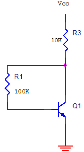
Fig. 1 has stability factor S1
If the above circuit is changed to below circuit
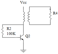
Fig. 2 having stability factor S2
Choose the correct option which is having better stability with S1 and S2 Values.
a) S2 = 151, S1 = 150. Circuit 1 has better stability
b) S2 = 100, S1 = 10 Circuit 2 has better stability
c) S2 = 151, S1 = 10.3 Circuit 1 has better stability
d) S2 = 151, S1 = 10.3 Circuit 2 has better stability
View Answer
Explanation: The above circuits are a collector to base bias circuits, where stability factor
\(S = \frac{1+β}{\frac{1+βR_C}{R_C+R_B}}\)
Thus, in the question, S1 =\( \frac{1+150}{1 + \frac{150*10}{110}} = \frac{151}{14.63}\) = 10.32
However, in circuit 2, which is a transformer coupled amplifier, RC = 0
Thus, S2 = 1+150 = 151.
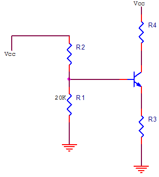
3. Consider the biasing circuit shown. The β for the circuit is large. R3 = 1kΩ, R4 = 2kΩ. The stability factor varies between 10 and 11. Find the maximum and minimum values of R2.
a) Minimum = 16.36kΩ, Maximum = 20kΩ
b) Minimum = 16.36kΩ, Maximum = 18kΩ
c) Minimum = 10 kΩ, Maximum = 20kΩ
d) Minimum = 6 kΩ, Maximum = 10kΩ
View Answer
Explanation: Circuit is a self bias circuit.
Base resistance = RB = R1*R2 / (R1+R2)
Since β is large, stability factor, S = 1 + RB/RE = 1 + RB/R3
1 + RB/R3 = 10
RB/R3 = 9 => RB = 9k => R2 = 16.36 kΩ
For S = 11
RB/R3=10 => RB = 10k => R2 = 20kΩ.
4. Choose the incorrect option according to self bias circuit?
a) Voltage gain increases
b) Stability factor is independent of collector resistance
c) BJT can be used in either of the three configurations
d) Excellent stability in collector current is achieved
View Answer
Explanation: In a self bias circuit, due to emitter resistance a negative feedback exists. This decreases voltage gain. Also, stability factor S does not depend on collector resistance, only on base and emitter resistance and β, if required. \(S = \frac{(1+β)(R_B +R_E)}{R_B + (1+β)R_E}\).
S is least in self bias circuit, hence excellent stability is achieved.
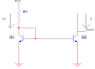
5. In the circuit given, the two Si transistors are similar. Given β=50, Vcc=12V, I1=5mA. Find I?
a) 5 mA
b) 4.807 mA
c) 4.5 mA
d) 5.2 mA
View Answer
Explanation: The circuit is a current mirror circuit. Both transistors are similar. I1= IREF = 5 mA
Β is not large so 2/β is not negligible.
Thus current I = I1/(1 + 2/β) = 5mA/(1 + 2/50) = 4.807 mA.
6. Given Vout = 5V, β=100, I1=10mA, R1=100KΩ. Find the output resistance.
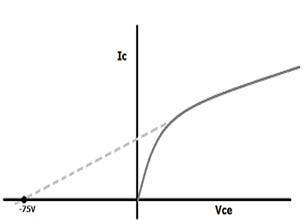
a) 8 kΩ
b) 8.163 kΩ
c) 7.582 kΩ
d) 8.4 kΩ
View Answer
Explanation: The circuit is a current mirror, whose output resistance, ROUT = (VA + VCE)/IOUT
Here, IOUT = I1 / (1+ 2/β) = 10mA / (1 + 2/100) = 9.8 mA
VCE = VOUT = 5V
VA = Early voltage = 75 V (obtained from the graph)
ROUT = (VA + VCE)/ IOUT = (75 + 5) / 9.8 * 10-3
ROUT = 80,000/9.8 = 8.163 kΩ.
7. Why is self bias circuit not used in IC amplifier?
a) To reduce power losses
b) To reduce area used on the chip
c) Stability factor reduces in the IC
d) Voltage gain is reduced
View Answer
Explanation: Self biased circuits are not preferred in IC amplifiers because they need large resistances R1 and R2, since then S will be smaller and stability will be more. However, using large resistances in ICs means a requirement of larger chip area, so to reduce this area requirement, we use current mirror circuits instead.
8. Considering all transistors to be similar and β is very large, when I1 = 10 mA, find current I2.
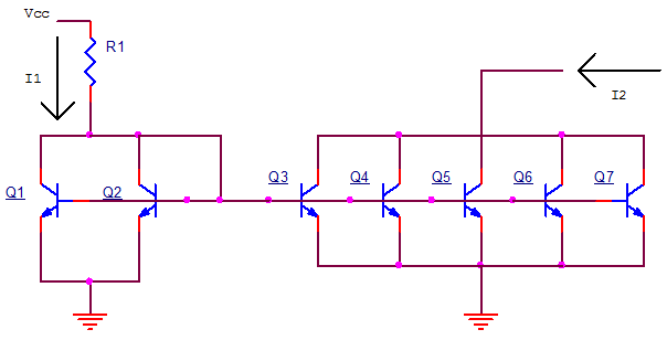
a) 10 mA
b) 50 mA
c) 25 mA
d) 20 mA
View Answer
Explanation: Let current through the transistor Q1/Q2 be IC. Since both are similar, we can say that,
IC = I1/2
Similarly, current through transistors Q3 to Q7 is assumed to be IC’, where IC’ = I2/5
Since all transistors are similar. IC = IC’
I2 = 5IC’ = 5 IC = 2.5*I1.
9. Consider the following circuit, where the transistors are similar Si transistors. Given I1 = 2mA, I2 = 1μA, Vcc = 12 V, find R1 and R2.
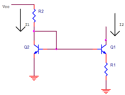
a) R1 = 10kΩ, R2 = 6kΩ
b) R1 = 5.6kΩ, R2 = 20kΩ
c) R1 =18kΩ, R2 = any value
d) R1 = 18kΩ, R2 = 5.6kΩ
View Answer
Explanation: R2 = (Vcc – VBE)/I1 = (12 – 0.7)/2m = 5.65 kΩ – Using KVL
Also, I2*R1 = VT ln(I1/I2) = 0.026 * ln(2)
Thus, R1 = 0.026*ln(2)/1μ = 18 kΩ.
10. Widlar current source was introduced to obtain a smaller output current.
a) True
b) False
View Answer
Explanation: In a current mirror circuit, to obtain lower values of output current, the resistance values required to increase a lot, which becomes difficult to manufacture on an IC. Instead, we use a widlar current source, where an emitter resistance is also present, affecting the output current.
Sanfoundry Global Education & Learning Series – Analog Circuits.
To practice all areas of Analog Circuits, here is complete set of 1000+ Multiple Choice Questions and Answers.
If you find a mistake in question / option / answer, kindly take a screenshot and email to [email protected]
