This set of Analog Circuits Multiple Choice Questions & Answers (MCQs) focuses on “MOSFET Amplifier with CG Configuration – 1”.
1. In the following circuit, what is the voltage at the source of the M1?
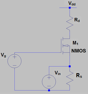
a) Vin * Rs / (Rs + 1/gm)
b) Vin * Rs / (Rs + gm)
c) Vin * Rs / (Rs – 1/gm)
d) Vin * Rs / (Rs + 2/gm)
View Answer
Explanation: The impedance looking into the source of M1 is 1/gm. Vin experiences a potential divider before entering the source of M1. The voltage drop across Rs is typically the voltage at the source and hence, it is equal to Vin * Rs / (Rs + 1/gm).
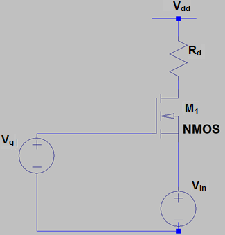
2. What is the input impedance of the following CG stage?
a) 1/gm
b) 2* Rs || 1/gm
c) Rs || 1/gm
d) Rs || 2/gm
View Answer
Explanation: The input impedance can be calculated by performing a small signal analysis at the input node. We need to set Vg and Vdd to 0V and apply a small input voltage at the source. Now, the impedance looking into the source is 1/gm and Rs is parallel to this impedance. Hence, the total input impedance is Rs || 1/gm.
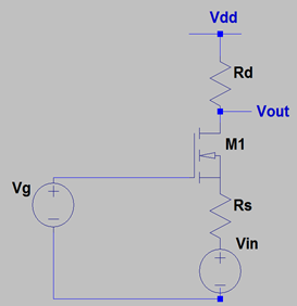
3. If Channel Length modulation is neglected, what is the voltage gain from the source to the drain for the CG stage shown below?
a) gm * Rd * {2Rs / (Rs + 1/gm)}
b) gm * Rd * {Rs / (Rs + 2/gm)}
c) gm * Rd * {2Rs / (Rs – 1/gm)}
d) gm * Rd * {Rs / (Rs + 1/gm)}
View Answer
Explanation: The voltage gain from the source of M1 to the drain of M1 can be found out from a small signal analysis and it’ll turn out to be gm * Rd. But the input voltage is a result of the potential divider between Rs and 1/gm. Hence, the overall voltage gain is gm * Rd * {Rs/ (Rs + 1/gm)}.
4. What is the input impedance for the following circuit?
a) ro
b) 1/gm
c) Rd || ro
d) Infinite
View Answer
Explanation: The input to the CG stage is placed at the source of M1. The impedance looking into the node of M1 is simply 1/gm. Hence, the input impedance is 1/gm. Rd || ro is the output impedance if channel length modulation is present.
5. If channel length modulation is neglected, what is the voltage gain for the following circuit from source to drain?
a) gm * Rd
b) gm * ro
c) gm * (ro || Rd)
d) -gm * Rd
View Answer
Explanation: In absence of channel length modulation, ro=0. The gain is simply gm * Rd. It should be noted that the CG stage doesn’t invert and hence the voltage gain is not -gm * Rd.
6. If channel length modulation is present, what is the output impedance of the following circuit?
a) Rd
b) Rd || ro
c) ro
d) 0
View Answer
Explanation: In presence of channel length modulation, ro appears to be in parallel to Rd. Hence, the total output impedance becomes Rd || ro. In the absence of channel length modulation, the output impedance is Rd only.
7. If channel length modulation is neglected, what is the voltage gain for the following CG stage?
a) Rd/(1/gm – Rs)
b) Rd/(3/gm + Rs)
c) Rd/(1/gm + Rs)
d) Rd/(2/gm + Rs)
View Answer
Explanation: The above circuit is quite similar to the CS stage with degeneration. But the CG stage doesn’t invert and after performing a small signal analysis, the voltage gain comes out to be Rd/(1/gm + Rs).
8. If channel length modulation is present. what is the overall output impedance of the following CG stage?
a) Rd || {Rs*(1+gm * ro) + ro}
b) Rd || {Rs*(1+gm * ro) + 2ro}
c) Rd || {Rs*(1+gm * ro) – ro}
d) Rd || {Rs*(2+gm * ro) + ro}
View Answer
Explanation: The impedance looking into the drain of M1 would be similar to that of a CS stage with source degeneration. That implies the impedance is Rs*(1+gm * ro) + ro. But this impedance is parallel to Rd. Hence, the overall output impedance becomes Rd || {Rs*(1+gm* ro) + ro}.
9. The current gain of a simple CG stage is approximate ____________
a) Infinity
b) unity
c) twice
d) 0
View Answer
Explanation: The input to a CS stage is at the source of M1. This current simply flows into the channel and flows out of M1. Approximately, we can say that the overall current gain is unity since the gain contributes very low current.
10. The voltage gain of a simple CG stage is greater than that of a follower.
a) True
b) False
View Answer
Explanation: The voltage gain of a follower is always less than that of a CG stage. This can be proven by a small signal analysis that the voltage gain for a follower is Rs/(1/gm + Rs) while that of the CG stage is gm * Rd. Hence the above statement is true.
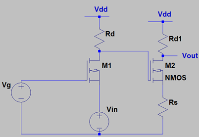
11. If channel length modulation is neglected, what is the voltage gain of the following circuit?
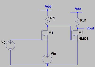
a) – {gm1 * Rd * gm2 * Rd1}
b) gm1 * Rd * gm2 * 2Rd1
c) – {gm1 * Rd * 2gm2 * Rd1}
d) gm1 * 2Rd * gm2 * Rd1
View Answer
Explanation: This is a cascade of a CG stage preceding a CS stage. For the CG stage, the voltage gain is gm * Rd. But after this stage, the signal gets amplified by the CS stage with a factor of –(gm2* Rd1). Hence, the overall voltage gain is the product of both the factors ie –(gm1 * Rd * gm2 * Rd1). Note that since channel length modulation is absent, ro is not present in the expression of gain.
12. If channel length modulation is present, what is the voltage gain of the following circuit?
a) gm1 * (Rd || ro1) * gm2 * Rd1
b) – {gm1 * Rd * gm2 * 2(Rd1 || ro2)}
c) – {gm1 * (Rd || ro1) * gm2 * (Rd1 || ro2)}
d) gm1 * 2Rd * gm2 * Rd1
View Answer
Explanation: This is a cascade of a CG stage preceding a CS stage. For the CG stage, the voltage gain is gm * (Rd || ro1). But after this stage, the signal gets amplified by the CS stage with a factor of – {gm2 * (Rd1 || ro2)}. Hence, the overall voltage gain is the product of both the factors i.e. – {gm1 * (Rd || ro1) * gm2 * (Rd1 || ro2)}. Note that the input impedance looking into M2 is infinite ad hence the voltage gain of the CG stage is typically unaffected by the CS stage (for low frequency operations only).
13. If channel length modulation is neglected, what is the voltage gain for the following circuit?
a) – {gm1 * Rd * Rd / (1/gm2 + Rs)}
b) – (gm1 * 2Rd * Rd / Rs)
c) – {gm1 * Rd * Rd / (1/gm2 + Rs)}
d) – {gm1 * Rd * Rd / (1/gm2 + 2Rs)}
View Answer
Explanation: This is a cascade of a CG stage preceding a CS stage. For the CG stage, the voltage gain is gm * Rd. But after this stage, the signal gets amplified by a degenerated CS stage with a factor of -Rd / (1/gm2 + Rs). Hence, the overall voltage gain is the product of both the factors i.e. – {gm1 * Rd * Rd / (1/gm2 + Rs)}. Note that the input impedance looking into M2 is infinite ad hence the voltage gain of the C.G. stage remains unaffected by the C.S. stage (for low frequency operations only).
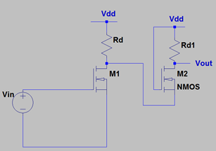
14. If channel length modulation is neglected, what is the overall voltage gain of the following circuit?
a) – {gm1 * (Rd || 1/gm2) * (Rd1/ (1/gm2 + Rd))}
b) – {gm1 * (Rd || 1/gm2) * gm2 * 2Rd1}
c) – {gm1 * Rd * gm2 * Rd1}
d) – {gm1 * 1/gm2 * gm2 * Rd1}
View Answer
Explanation: This is a cascade of CS stage preceding a CG stage. The voltage gain of the first stage is – (gm1 * Rd || 1/gm2). This is because the drain of M1 is connected to the source of M2 and the impedance looking into the source of M2 is 1/gm2. Now, the source of the CG stage is connected to Rd and hence the voltage gain due to this stage is affected by source degeneration and the voltage gain is Rd1/ (1/gm2 + Rd). The overall voltage gain is – {gm1 * (Rd || 1/gm2) * (Rd1/ (1/gm2 + Rd))}.
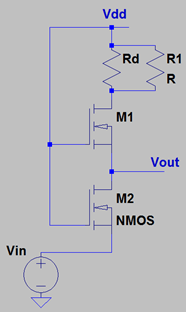
15. If channel length modulation is neglected, what is the voltage gain of the following circuit?
a) gm2/gm1
b) – {gm2 * Rd * gm1 * R1}
c) Rd/gm2
d) 0
View Answer
Explanation: The impedance looking into the source of M1 is 1/gm1. Hence, the product of this times the transconductance of M2 will be the overall voltage gain i.e. gm2/gm1. Note that the gain is function of only the intrinsic parameters of the MOSFET and independent of other parameters.
Sanfoundry Global Education & Learning Series – Analog Circuits.
To practice all areas of Analog Circuits, here is complete set of 1000+ Multiple Choice Questions and Answers.
If you find a mistake in question / option / answer, kindly take a screenshot and email to [email protected]
