This set of Analog Circuits Multiple Choice Questions & Answers (MCQs) focuses on “MOSFET Amplifier with CD Configuration – 1”.
1. If channel length modulation is present, what is the voltage gain?
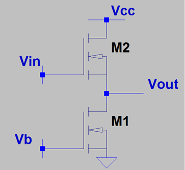
a) ro1 / {(1/gm1 || ro2) + ro1}
b) ro2 / (1/gm1 + ro1)
c) ro2 / (1/gm1 + 3ro2)
d) ro2 / (2/gm1 + ro2)
View Answer
Explanation: M2 behaves as a Source follower i.e. it is being used in a C.D. configuration. M1 provides a output resistance of ro1 but M2 provides an impedance of (1/gm2||ro2). Thus, from the voltage gain of a follower stage, we conclude the overall voltage gain is ro1 / {(1/gm1 || ro2) + ro1}.
2. If channel length modulation is present, what is the impedance looking into node X?
a) (1/gm2 || ro2 || 1/gm1)
b) (1/gm2 || 1/gm1 || ro1)
c) (1/gm2 || ro2 || 12/gm1 || ro1)
d) (1/gm2 || ro2 || 1/gm1 || ro1)
View Answer
Explanation: The source of M1 and M2 are connected at node X. The impedance looking into the source of a MOSFET is (1/gm || ro). If we look at node X, M1 and M2 are connected from Node X to ground. Hence, they are parallel to each other and the overall impedance becomes (1/gm2 || ro2 || 1/gm1 || ro1).
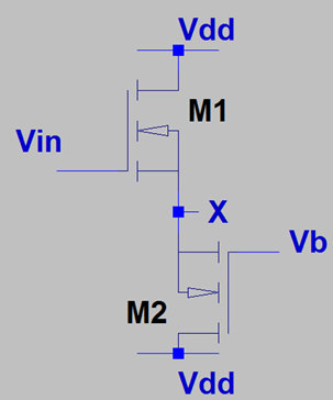
3. If channel length modulation is present in M1 but not in M2, what is the voltage gain at node X?
a) (1/gm2 || ro2) / {1/gm2 + ( 1/gm1 || ro1)}
b) (1/gm1 || ro1) / (1/gm2 + ro1)
c) 1/gm1 / (1/gm2 + 1/gm1)
d) 1/gm1 / {1/gm2 + (1/gm1 || ro1)}
View Answer
Explanation: The voltage gain at node X is due to M1 being used in the CD configuration. Since M1 offers channel length modulation but not M2, we note that the impedance looking into the source of M2 is 1/gm2 but for M1, it’s (1/gm2 || ro2). From the voltage gain of a follower stage, we conclude that the voltage gain is (1/gm2 || ro2) / {1/gm1 + ( 1/gm1 || ro1)}.
4. The follower stage provides _____ input impedance.
a) low
b) equal
c) very high
d) very low
View Answer
Explanation: The input to the follower stage is applied to the gate of the MOSFET. The gate of the MOSFET is made of Si02, which is a dielectric and provides very high impedance to the input.
5. The output impedance of the follower is _____________
a) Low
b) Very low
c) Depends on it’s transconductance and low
d) High
View Answer
Explanation: The output impedance of the follower is a function of the transconductance. But it’s also a function of the channel length modulation. But the resistance offered due to channel length modulation is much greater than the inverse of the transconductance. It can be concluded that the output of the follower depends on the transconductance and it’s low.
6. The follower stage is mostly used as a ____________
a) Current source
b) Buffer stage
c) Amplifier
d) Switch
View Answer
Explanation: The C.D. configuration offers high input impedance to the input signal and low output impedance while sensing the output signal. Thus, it is used as a buffer stage.
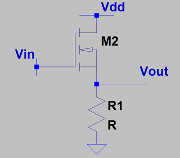
7. Assume µnCox = 100 µA/V2 and supply current is 5mA, what should be the aspect ratio so that a 50 Ω load can be used to give a voltage gain of .25 in C.D. configuration?
a) 32.6
b) 50
c) 40
d) 41
View Answer
Explanation: The voltage gain is given by RL/(1/gm + RL) where RL is the 50 Ω load. Now, we see that if the voltage gain is .25, gm is 1/175. Now, gm is \(\sqrt{(2* µ_nC_{ox} * (W/L) * Id)}\) where (W/L) is the aspect ratio, Id is the drain current. We have all the values and the aspect ratio becomes 32.6.
8. If maximum power is transferred to the load R1, the transconductance is .02 and channel length modulation is neglected, what should be the value of the load?
a) 50 Ω
b) 32 Ω
c) 16 Ω
d) 10 Ω
View Answer
Explanation: Since the transconductance is .02, it’s inverse is 50. From the general expression of voltage gain of a source follower, we conclude that the load should be 50 Ω since the inverse of the transconductance is the impedance looking into the source of the MOSFET. For maximum power transfer, we have to match both the impedance.
9. If g is the transconductance and r is the resistance due to channel length modulation – what is the total voltage gain if only M1 has channel length modulation?
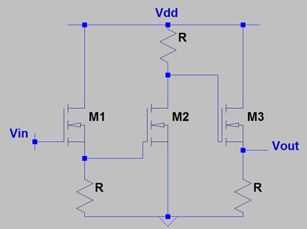
a) R / ((1/g || r ) + R) * g *R * R / (1/g + R)
b) R / ((1/g || r ) + R) * g *R * R * g
c) R / ((1/g || r )) * g *R * R / (1/g + R)
d) R / ((1/g ) + R) * g *R * R / (1/g + R)
View Answer
Explanation: This is a cascade of a follower stage follower by a CS stage which precedes another follower stage. The gain due to each stage gets multiplied until we reach the output. For the first stage, the gain is R/ ((1/g || r)+ R) since M1 has channel length modulation. The second stage has a gain of g * R while the final stage has a gain of R/ (1/g + R). After multiplying the gains, we get R/ ((1/g || r )+ R) * g *R * R/ (1/g + R).
10. If g is the transconductance and r is the resistance due to channel length modulation – what is the total voltage gain if both M2 and M3 has channel length modulation?
a) R/ ((1/g || r) + R) * g * (R || r) * R * g
b) R/ ((1/g + R) * g * (R || r) * R/ ((1/g || r) + R)
c) R/ ((1/g || r)) * g *R * R/ ((1/g || r) + R)
d) R/ ((1/g ) + R) * g *R * R *2g
View Answer
Explanation: This is a cascade of a follower stage follower by a CS stage which precedes another follower stage. The gain due to each stage gets multiplied until we reach the output. For the first stage, the gain is R / ((1/g+ R). The second stage has a gain of g * (R || r) while the final stage has a gain of R/ ((1/g || r) + R)- the effect of r is simply due to channel length modulation. After multiplying the gains, we get R/ ((1/g + R) * g * (R || r) * R/ ((1/g || r) + R).
11. If g is the transconductance and r is the resistance due to channel length modulation – what is the total voltage gain if both M1 and M3 has channel length modulation?
a) R / ((1/g || r) + R) * g * R * R / ((1/gm || r))
b) R / ((1/g + 4R) * g * R / ((1/g || r) + 3R)
c) R / ((1/g || r)) * g *R * R / ((1/g || r) + 2R)
d) R / ((1/g) * R * R * g * 4g
View Answer
Explanation: This is a cascade of a follower stage follower by a CS stage which precedes another follower stage. The gain due to each stage gets multiplied until we reach the output. For the first stage, the gain is R/ ((1/g || r) + R). The second stage has a gain of g * R while the final stage has a gain of R/ ((1/g || r) + R). The presence of r is due to channel length modulation. After multiplying the gains, we get R/ ((1/g || r) + R) * g * R * R / ((1/gm || r)).
12. Neglecting Channel Length Modulation, if the transconductance of the MOSFET increases, the gain of the follower stage will _________
a) decreases
b) increases
c) doesn’t get affected
d) doubles
View Answer
Explanation: The gain of the follower stage is given by Rs/(1/gm + Rs). Hence, we readily conclude that if the transconductance (gm) increases, the gain will increase.
13. Neglecting Channel Length Modulation, if the aspect ratio of the MOSFET increases, the gain of the follower stage will _________
a) increase
b) decrease
c) increases proportionately
d) doesn’t get affected
View Answer
Explanation: The square root of the aspect ratio is directly proportional to the transconductance of the MOSFET. If it increases, the transconductance increases and hence according to the expression of the voltage gain of a follower stage gain increases.
14. Neglecting Channel Length Modulation, if the transconductance increases, the input impedance of a follower stage ___________
a) Remans the same
b) Increases
c) Decreases
d) Doubles
View Answer
Explanation: The input impedance is extremely high for a follower stage because the input is applied to the gate of the MOSFET. The SiO2 layer is the primary reason for such a high impedance value.
15. Neglecting Channel Length Modulation, if the transconductance of a MOSFET increases, the output impedance of the follower stage can _________
a) increase
b) decrease
c) increase linearly
d) decrease non-linearly
View Answer
Explanation: The output impedance of a follower stage is (1/gm || Rd). If the transconductance increases, the output impedance will decrease, as can be seen from the formulae.
Sanfoundry Global Education & Learning Series – Analog Circuits.
To practice all areas of Analog Circuits, here is complete set of 1000+ Multiple Choice Questions and Answers.
If you find a mistake in question / option / answer, kindly take a screenshot and email to [email protected]
- Check Analog Electronics Books
- Apply for Electrical Engineering Internship
- Practice Electrical & Electronics Engineering MCQs
- Apply for Electrical & Electronics Engineering Internship
- Practice Electrical Engineering MCQs
