This set of Analog Circuits Multiple Choice Questions & Answers (MCQs) focuses on “Characteristics of Amplifier”.
1. The state amplifier has no input is not called ______________
a) Zero signal condition
b) Non-signal condition
c) Quiescent condition
d) Empty-signal condition
View Answer
Explanation: The state at which amplifier has zero input signal is called zero signal condition, Non-signal condition, quiescent condition. There is nothing named empty-signal condition.
2. Which of the following is not considered for quiescent operating point?
a) DC collector-emitter voltage
b) DC collector current
c) DC base current
d) DC input voltage
View Answer
Explanation: The quiescent point is the operating point of an amplifier where the DC condition of amplifier is constant. For that we have to make sure that DC collector-emitter voltage, DC collector current, DC base current are constant.
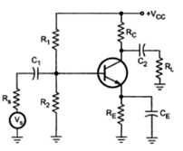
3. Which of the following resistor is not involving in biasing the circuit shown below?

a) R1
b) R2
c) RC
d) RL
View Answer
Explanation: R1, R2, RC are, used to bias the circuit while RL is used as a load resistor. R1, R2 are used as a voltage divider. RC is used to control collector current.
4. Which of the following statements is most correct to explain role of biasing circuit in the implementation of a transistor circuit?
a) It is used provide proper voltage to every component in the circuit
b) It is used to ensure maximum power is obtained out of the circuit
c) It is used to provide the quiescent collector current
d) It is used to provide proper and stable functional environment to all quiescent point parameters
View Answer
Explanation: The basic function of biasing is to maintain amplifier in quiescent condition. The amplifier will properly work only if the quiescent condition is stable.
5. What is the role of input capacitance in the transistor amplifying circuit?
a) To prevent input variation from reaching output
b) To prevent DC content in the input from reaching transistor
c) There isn’t any role for input capacitance
d) To increase input impedance
View Answer
Explanation: The input capacitance, as its name indicates is used to prevent DC offset voltages in the input. It also prevents the transistor bias voltage to be fed back to input generating circuit.
6. What is the role of emitter bypass capacitance in the transistor amplifying circuit?
a) To prevent damage of emitter resistance from variation in voltage
b) To prevent emitter from over voltage
c) To increase gain
d) To increase load to transistor circuit
View Answer
Explanation: When an emitter resistance is added to the amplifier circuit, in common emitter mode, voltage gain is reduced and input impedance increases. When we need to obtain higher gain, we add a capacitance in parallel to the emitter resistance, called emitter bypass capacitance, and voltage gain does not decrease.
7. Which of the following is actually not a function of emitter bypass capacitor?
a) Increase gain
b) Lower the impedance of emitter resistance
c) Provide a low reactance path
d) Help emitter resistance to withstand voltage variation
View Answer
Explanation: The emitter bypass capacitor is not meant for reducing loading effect of emitter resistance. It is to increase gain. It provides a low reactive path to the AC signal without changing the quiescent point.
8. What is the role of emitter resistance in the transistor amplifying circuit?
a) To prevent thermal runaway
b) To prevent increase in gain
c) To lower the output impedance
d) To increase gain
View Answer
Explanation: Thermal runaway is the increase in the collector current without an increase in input due to heating of semiconductor material which in turn reduce the resistance thus increases current. The emitter resistor decreases effective input voltage decrease when collector current increases and thus it reduces collector current itself.
9. Which of the following is not true regarding the output capacitor in the transistor biasing circuit?
a) To pass AC signal
b) To stop DC signal
c) To couple the amplifier to load or next amplifier
d) There is no importance for an output capacitance
View Answer
Explanation: The output capacitor or output coupling capacitor is provided to pass AC signal and to block DC signal. It also helps to couple the amplifier to load or next amplifier.
10. Which of the following is the best biasing method for transistor bias?
a) emitter bias
b) voltage divider bias
c) fixed bias
d) collector feedback bias
View Answer
Explanation: Voltage divider bias is more stable because the biased voltage will not change. It is best to use voltage divider bias for accuracy.
Sanfoundry Global Education & Learning Series – Analog Circuits.
To practice all areas of Analog Circuits, here is complete set of 1000+ Multiple Choice Questions and Answers.
If you find a mistake in question / option / answer, kindly take a screenshot and email to [email protected]
- Check Analog Electronics Books
- Check Electrical & Electronics Engineering Books
- Apply for Electrical Engineering Internship
- Apply for Electrical & Electronics Engineering Internship
- Practice Electrical Engineering MCQs
