This set of Microelectronics Multiple Choice Questions & Answers (MCQs) focuses on “MOS Cascode – Set 2”.
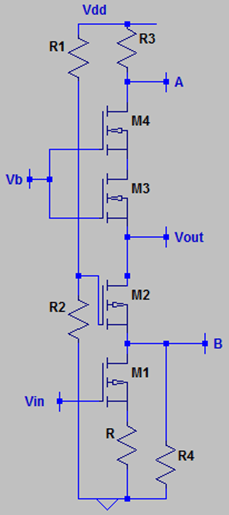
1. What is the impedance looking into the drain of M3 in presence of channel length modulation & body effect?
a) [1+(gmb3+gm3)*ro4)]*ro4+ro3
b) [1+(gmb4+gm4)*ro3)]*ro4+ro3
c) [1+(gmb3*ro3)]*([1+(gm4*ro4)]*R3+ro4)+ro3
d) [1+(gmb4*ro3)]*ro4+ro3
View Answer
Explanation: M3 is a PMOS and is degenerated by M4. M4 is also a PMOS and is degenerated by R3 and it offers an output resistance of [1+(gm4*ro4)]*R3+ro4 to the source of M3. Hence, the impedance looking into the drain terminal of M3 will be [1+(gmb3*ro3)]*([1+(gm4*ro4)]*R3+ro4)+ro3. Note that the circuit below the drain terminal will not affect the impedance. This impedance can be verified by the small signal analysis.
2. What is the impedance looking into the drain of M2 in presence of channel length modulation & body effect?
a) [1+(gmb3*ro4)]*ro4+ro3
b) [1+(gmb2+gm2)*ro2]*([{1+(gm1*ro1)}*R+ro1]||R4)+ro2
c) [1+(gmb2*ro2)]*([{1+(gm1*ro1)}*R+ro1]||R4)+ro2
d) [1+(gmb2+gm2)*ro2]*([{1+(gm1*ro1)]*R+ro1)+ro2
View Answer
Explanation: M2 is a NMOS and is degenerated by M1. M1 is also a NMOS and is degenerated by R and it offers an output resistance of [{1+(gm1*ro1)}*R+ro1 to the source of M2. This impedance is in parallel to R4. The total impedance degenerating M2 is [1+(gm1*ro1)*R+ro1]||R4. Hence, the impedance looking into the drain terminal of M3 will be [1+(gmb2+gm2)*ro2]*([{1+(gm1*ro1)}*R+ro1]||R4)+ro2. Note that the circuit above the drain terminal will not affect the impedance.
3. What is the output impedance of the following circuit if all the MOSFETs suffer from channel length modulation & body effect?
a) [1+(gmb3*ro3)]*([1+(gm4*ro4)]*R3+ro4)+ro3||[1+(gmb2+gm2)*ro3]*([{1+(gm2*ro1)}*R+ro2]||R3)+ro1
b) [1+(gmb1*ro1)]*([1+(gm2*ro4)]*R2+ro3)+ro3||[1+((gmb1+gm2)*ro4]*([{1+(gm1*ro1)}*R+ro1]||R4)+ro2
c) [1+(gmb2*ro3)]*([1+(gm2*ro3)]*R4+ro3)+ro3||[1+(gmb2+gm2)*ro2]*([{1+(gm1*ro1)}*R+ro1]||R4)+ro2
d) [1+(gmb3*ro3)]*([1+(gm4*ro4)]*R3+ro4)+ro3||[1+(gmb2+gm2)*ro2]*([{1+(gm1*ro1)}*R+ro1]||R4)+ro2
View Answer
Explanation: At the output node, we have primarily two branches. One branch is connected to a degenerated PMOS M3, degenerated by M4, which offers an output impedance of [1+(gmb3*ro3)]*([1+(gm4*ro4)]*R3+ro4)+ro3. Another branch is connected to a degenerated NMOS M2, degenerated by a degenerated M1, which offers an output impedance of [1+(gmb2+gm2)*ro2]*([{1+(gm1*ro1)}*R+ro1]|| R4)+ro2. These two impedance appear in parallel to each other and the overall output impedance is [1+(gmb3*ro3)]*([1+(gm4*ro4)]*R3+ro4)+ro3||[1+(gmb2+gm2)*ro2]*([{1+(gm1*ro1)}*R+ro1]||R4)+ro2.
4. What is the transconductance of M2 if all the MOSFETs suffers from Channel Length Modulation and body effect?
a) gm2*ro2/[[{1+(gm1*ro1)}*R+ro1]||R4]+[1+(gm2+gmb2)[[{1+(gm1*ro1)}*R+ro1]||R4]]ro2
b) gm1*ro1/[[{1+(gm1*ro1)}*R+ro1]||R4]+[1+(gm4+gmb4)[[{1+(gm1*ro1)}*R+ro1]||R4]]ro4
c) gm2*ro2/[[{1+(gm1*ro1)}*R+ro1]||R4]+[1+(gm3+gmb3)[[{1+(gm1*ro1)}*R+ro1]||R4]]ro3
d) gm3*ro3/[[{1+(gm1*ro1)}*R+ro1]||R4]+[1+(gm1+gmb3)[{1+(gm1*ro1)}*R+ro1]||R4]]ro3
View Answer
Explanation: We know that in presence of channel length modulation, body effect and a source resistance – the transconductance of an NMOS or PMOS is gm*ro/RS+[1+(gm+gmb)RS]ro. For M2, the source resistance is R4 in parallel to the output impedance of a degenerated M1. This comes out to be ro1 [{1+(gm1*ro1)}*R+ro1]||R4. Henceforth, for M2, the transconductance becomes gm2*ro2/[[{1+(gm1*ro1)}*R+ro1]||R4]+[1+(gm2+gmb2)[[{1+(gm1*ro1)}*R+ro1]||R4]]ro2. We can check the unit will come out to be Siemens and this can also be confirmed by a small signal analysis. Note that we are not concerned with the impedance connected to the drain of M2 for now. In absence of body effect, we omit the gmb terms.
5. What is the voltage gain of the following circuit if each MOSFET suffer from Channel Length Modulation & Body effect?
a) {(gmb+gm)*ro+1}[[1+(gmb3*ro3)]*([1+(gm4*ro4)] * R3+ro4) + ro3||[1+(gmb2+gm2)*ro2] * ([{1+(gm1*ro1)} * R++[[{1+(gm1*ro1)}*R+ro1]]+[[1+(gmb3*ro3)]*([1+(gm4*ro4)]*R3+ro4)+ro3||[1+(gmb2+gm2)*ro2]*([{1+(gm1*ro1)}*R+ro1]||R4)+ro2)]
b) {(gmb+gm)*ro+1}[[1+(gmb3*ro3)]*([1+(gm4*ro4)] * R3+ro4)+ro3||[1+(gmb2+gm2)*ro2]*([{1+(gm1*ro1)}*R++[[{1+(gm1*ro1)}*R+ro1]]+[[1+(gmb3*ro3)]*([1+(gm4*ro4)]*R3+ro4)+ro3||[1+(gmb2+gm2)*ro2]*([{1+(gm1*ro1)}*R+ro1]||R4)+1)]
c) {(gmb3+gm1)*ro+1}[[1+(gmb2*ro3)]*([1+(gm4*r04)] * R3+ro4)+ro1]||R4)+ro2]/(ro+(gmb+gm)*ro[[{1+(gm1*ro1)}*R+ro3]]+[[{1+(gm1*ro1)}*R+ro1]]+[[1+(gmb3*ro3)]*([1+(gm4*ro4)]*R3+ro4)+ro3||[1+(gmb2+gm2)*ro2]*([{1+(gm1*ro2)}*R+ro1]||R4)+ro2)]
d) {(gmb2+gm2)*ro2+1}[[1+(gmb3*ro3)]*([1+(gm4*ro4)] * R3+ro4)+ro3||[1+(gmb2+gm2)*ro2] * ([{1+(gm1*ro1)} * R+ro1]||R4)+ro2]/(ro2+(gmb2+gm2)*ro2[[{1+(gm1*ro1)}*R+ro1]]+[[{1+(gm1 * ro1)}*R+ro1]]+[[1+(gmb3*ro3)]*([1+(gm4*ro4)]*R3+ro4)+ro3||[1+(gmb2+gm2)*ro2]*([{1+(gm1*ro1)}*R+ro1]||R4)+ro2)]
View Answer
Explanation: We analyze this circuit by observing that the output is taken from the drain of M2 which behaves as a CG stage. In presence of Body effect and Channel Length modulation, the voltage gain of a CG stage is {(gmb+gm)*ro+1}RD/(ro+(gmb+gm)*roRS+RS+RD). Now, RD is the total impedance connected to the drain of M2 & it is the output impedance at the drain terminal. This resistance comes out to be [1+(gmb3*ro3)]*([1+(gm4*ro4)]*R3+ro4)+ro3||[1+(gmb2+gm2)*ro2]*([{1+(gm1*ro1)}*R+ro1]||R4)+ro2]. Moreover, the source resistance is [{1+(gm1*ro1)}*R+ro1]. Now, we simply replace RD & RS & the overall voltage gain comes out to be {(gmb2+gm2)*ro2+1}[[1+(gmb3*ro3)]*([1+(gm4*ro4)]*R3+ro4)+ro3||[1+(gmb2+gm2)*ro2]*([{1+(gm1*ro1)}*R+ro1]||R4)+ro2]/(ro2+(gmb2+gm2)*ro2[[{1+(gm1*ro1)}*R+ro1]]+[[1+(gmb3*ro3)]*([1+(gm4*ro4)]*R3+ro4)+ro3||[1+(gmb2+gm2)*ro2]*([{1+(gm1*ro1)}*R+ro1]||R4)+ro2)]. We note that the expression is very long & we can always use some approximations to calculate the voltage gain.
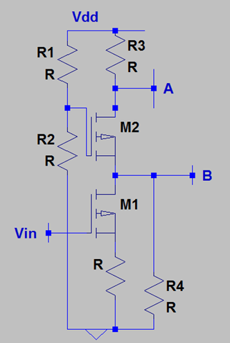
6. What is the voltage gain from node B to node A in presence of Channel Length Modulation & Body Effect?
a) {(gm1+gmb1)ro1+1}/ro2+(gm2+gmb1)*ro2*([1+(gm2+gmb2)ro1]R+ro1||R3)+([1+(gm2-gmb2)ro1]R+ro1||R4)+R3
b) {(gm2+gmb2)ro2+1}/ro2+(gm2+gmb2)*ro2*([1+(gm2+gmb2)ro1]R+ro1||R4)+([1+(gm2+gmb2)ro1]R+ro1||R4)+R3
c) {(gm1+gmb2)ro2+1}/ro1+(gm1+gmb2)*ro2*([1+(gm2+gmb2)ro1]R+ro1||R3)+([1+(gm2-gmb2)ro1]R+ro2||R4)+R3
d) {(gm2+gmb1)ro1+1}/ro1+(gm2+gmb2)*ro2*([1+(gm2+gmb2)ro1]R+ro1||R4)+([1+(gm2+gmb2)ro1]R+ro2||R4)+R3
View Answer
Explanation: From Node B to Node A, M2 plays the role of a CG stage. The total resistance connected to the source of M2 is a parallel combination of two impedances. The first is looking into the drain of M1 which is degenerated by R and in presence of channel length modulation & body effect, it becomes [1+(gm2+gmb2)ro1]R+ro1. The second impedance is R4. The overall impedance is [1+(gm2+gmb2)ro1]R+ro1||R4. The total resistance connected to the drain of M2 is R3. From the expression of Voltage gain of a CG stage, in presence of channel length modulation & Body effect, the voltage gain is {(gm2+gmb2)ro2+1}/ro2+(gm2+gmb2)*ro2*([1+(gm2+gmb2)ro1]R+ro1||R4)+([1+(gm2+gmb2)ro1]R+ro1||R4)+R3. Note that in absence of body effect, only gmb will disappear from the expression.
7. Which circuit is more linear?
Circuit: A Ciruit: B
a) Circuit A
b) Circuit B
c) It depends on the biasing
d) It depends on the supply voltage
View Answer
Explanation: Circuit B is more linear than circuit A since both the MOSFETs are degenerated & degeneration leads to linearization of the circuit.
8. What is the role of M4 in the following circuit?
a) Degenerating device
b) Input device
c) Amplifier
d) Error in the circuit
View Answer
Explanation: M4 plays the role of a degenerating device. It is connected to the source of M3 & it degenerates M3 which leads to an increase in the impedance of M3 which is seen looking into its drain terminal.
9. What is the voltage gain at Node B in presence of Channel length modulation and body effect in both the MOSFETs?
a) gm1*ro/R+[1+(gm1+gmb1)R]ro1*(R3+ro2)/(1+(gm2+gmb2)*ro2)||[1+(gm2+gmb2)ro1]R+ro1||R4
b) gm2*ro/R+[1+(gm2+gmb2)R]ro1*(R3+ro2)/(1+(gm2+gmb2)*ro2)||[1+(gm2+gmb2)ro1]R+ro1||R4
c) gm1*ro/R+[1+(gm2+gmb1)R]ro1*(R3+ro2)/(1+(gm2+gmb2)*ro2)||[1+(gm2+gmb2)ro1]R+ro1||R4
d) gm1*ro/R+[1+(gm1+gmb1)R]ro1*(R3+ro2)/(1+(gm2+gmb2)*ro2)||[1+(gm2+gmb2)ro1]R+ro1||R4
View Answer
Explanation: We analyze the circuit by observing that M1 behaves as a CS stage. The transconductance of M1 is gm*ro/R+[1+(gm+gmb)R]ro1. The output impedance of is the parallel combination of the three impedances. The first impedance is looking into the source of M2, which is (R3+ro2)/(1+(gm2+gmb2)*ro2). The second is looking into the drain of M1 which is degenerated by R and in presence of channel length modulation & body effect, it becomes [1+(gm2+gmb2)ro1]R+ro1. The final impedance is R4. The overall output impedance is (R3+ro2)/(1+(gm2+gmb2)*ro2)||[1+(gm2+gmb2)ro1]R+ro1||R4 & the voltage gain becomes gm1*ro/R+[1+(gm1+gmb1)R]ro1*(R3+ro2)/(1+(gm2+gmb2)*ro2)||[1+(gm2+gmb2)ro1]R+ro1||R4.
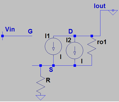
10. What is the transconductance of M1 in presence of Channel Length Modulation & Body effect?
a) gm2*ro2/R+[1+(gm2+gmb1)R]ro2
b) gm1*ro2/R+[1+(gm2+gmb2)R]ro1
c) gm1*ro1/R+[1+(gm1+gmb1)R]ro1
d) gm2*ro2/R+[1+(gm1+gmb2)R]ro2
View Answer
Explanation: In order to calculate the transconductance of M1, we analyze M1 by neglecting M2 since the current leaving the drain of M1 is independent of RD (the impedance of the branch connected to the drain terminal). Note that the voltage drop across RD plays a role in establishing the region of operation but the transconductance i.e. ΔID/ΔVGS is independent of RD. We draw the small signal model of M1 with channel length modulation and Body effect. Henceforth, we write a KCL at the source after noting that I2=gmb*VS=gmb*(IOUT*R) & I1=gm*VGS=gm*(Vin-IOUT*R) & Iro1=VS/ro1=IOUT*R/ro1. The KCL revel as IOUT=I1–I2–Iro1 & we replace the terms and rearrange to find the transconductance as gm*ro/R+[1+(gm+gmb)R]ro1.
Sanfoundry Global Education & Learning Series – Microelectronics.
To practice all areas of Microelectronics, here is complete set of 1000+ Multiple Choice Questions and Answers.
If you find a mistake in question / option / answer, kindly take a screenshot and email to [email protected]
