This is a PLC Program to Implement 1:8 Demultiplexer.
Problem Description
Implementing 1:8 De-multiplexer in PLC using Ladder Diagram programming language.
Problem Solution
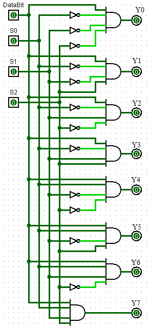
- It has one data input Di, three select input S0, S1 and S3 and 8 outputs Y0 to Y7.
- To select n outputs, we need m select lines such that 2^m = n. Depending on the output. The selection of one of the n outputs is done by the select pins.
- It does not need K-map and simplification so one step is eliminated to create Ladder Logic Diagram.
- Realize the de-multiplexer using Logic Gates.
- Truth Table can be written as given below.
Truth Table relating 1:8 De-Multiplexer
Data	Select Inputs	Output
Inputs	S2 S1 S0        Y7 Y6 Y5 Y4 Y3 Y2 Y1 Y0
Di	0  0  0	        0  0  0	 0  0  0  0  Di
Di	0  0  1	        0  0  0	 0  0  0  Di 0
Di	0  1  0	        0  0  0	 0  0  Di 0  0
Di	0  1  1	        0  0  0	 0  Di 0  0  0
Di	1  0  0	        0  0  0	 Di 0  0  0  0
Di	1  0  1	        0  0  Di 0  0  0  0  0
Di	1  1  0	        0  Di 0	 0  0  0  0  0
Di	1  1  1	        Di 0  0	 0  0  0  0  0
Realizing 1:8 De-Mux using Logic Gates
PLC Program
Here is PLC program to Implement 1:8 Demultiplexer, along with program explanation and run time test cases.
advertisement
advertisement
List of Inputs and Outputs
 S0=		I:1/0	(Select Line Input)
 S1=		I:1/1	(Select Line Input)
 S2=		I:1/2	(Select Line Input)
 Din=		I:1/3	(Data Input)
 Y0=		O:2/0	(Output)
 Y1=		O:2/1	(Output)
 Y2=		O:2/2	(Output)
 Y3=		O:2/3	(Output)
 Y4=		O:2/4	(Output)
 Y5=		O:2/5	(Output)
 Y6=		O:2/6	(Output)
 Y7=		O:2/7	(Output)
Ladder Diagram to obtain output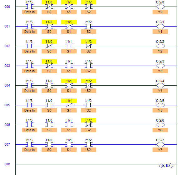
Program Description
- In all the rungs, S2 (I:1/0), S1 (I:1/1) and S0 (I:1/2) are used as a selector line input as shown in Logic Circuit.
- Y0 to Y7, O:2/7 are Onputs respectively.
- When S2 (I:1/0), S1 (I:1/1) and S0 (I:1/2) are low, Y0 output will have whatever state Data Input bit I:1/3 holds, either 1 or 0.
- When S2 (I:1/0) and S1 (I:1/1) are low and S0 (I:1/1) is high, Y1 output will have whatever state Data Input bit I:1/3 holds.
- Similarly remaining six different outputs are obtained.
- In other words, according to bit pattern of S2, S1 and S0, Data Input bit Din is passed to outputs Y0-Y7.
- Here, instead of outputs Y0 to Y7, any final control element can be operated depending upon the application.
Runtime Test Cases
Data    Select Inputs	Output
Inputs  S2 S1 S0        Y7 Y6 Y5 Y4 Y3 Y2 Y1 Y0
Di	0  0  0	        0  0  0	 0  0  0  0  Di
Di	0  0  1	        0  0  0	 0  0  0  Di 0
Di	0  1  0	        0  0  0	 0  0  Di 0  0
Di	0  1  1	        0  0  0	 0  Di 0  0  0
Di	1  0  0	        0  0  0	 Di 0  0  0  0
Di	1  0  1	        0  0  Di 0  0  0  0  0
Di	1  1  0	        0  Di 0	 0  0  0  0  0
Di	1  1  1	        Di 0  0	 0  0  0  0  0
Sanfoundry Global Education & Learning Series – PLC Algorithms.
To practice all PLC programs, here is complete set of 100+ PLC Problems and Solutions.
