This set of Logic Design Multiple Choice Questions & Answers (MCQs) focuses on “VHDL Description of Combinational Circuits”.
1. The acronym VHDL stands for VHSIC Hardware Description Language, and VHSIC in turn stands for Very High Speed Integrated Circuit.
a) True
b) False
View Answer
Explanation: The acronym VHDL stands for VHSIC Hardware Description Language, and VHSIC in turn stands for Very High Speed Integrated Circuit trance. A hardware description language allows a digital system to be designed and debugged at a higher level before implementation at the gate and flip-flop level.
2. In VHDL, to obtain synthesizable code, what is used to describe a hardware signal?
a) Signal
b) Variable
c) Architecture
d) Entity
View Answer
Explanation: VHDL signals are used to describe a signal in a physical system. The VHDL language also includes variables similar to variables in programming languages, but to obtain synthesizable code for hardware, signals should be used to represent hardware signals.
3. In general, VHDL is case sensitive.
a) True
b) False
View Answer
Explanation: In general, VHDL is not case sensitive, that is, capital and lowercase letters are treated the same by the compiler and the simulator. Thus, the statements
A <= B After 10 NS;
a <= b after 10 ns;
would be treated exactly the same.
4. In VHDL, what could an identifier start with?
a) Underscore or letter or number
b) Letter or number
c) Number or underscore
d) Letter
View Answer
Explanation: An identifier in VHDL must start with a letter only. If an identifier in VHDL does not start with a letter, the compiler will throw a syntax error.
5. In VHDL, what could an identifier end with?
a) Underscore or letter or number
b) Letter or number
c) Number or underscore
d) Letter
View Answer
Explanation: An identifier in VHDL cannot end with an underscore. If an identifier in VHDL ends with an underscore, the compiler will throw a syntax error.
6. Identify the correct VHDL statement for a clock with a frequency of 50 MHz. Let the signal be CLK.
a) CLK <= not CLK after 10 ns;
b) CLK <= not CLK after 20 ns;
c) CLK <= NOT CLK;
d) CLK <= NOT CLK after 1 ns;
View Answer
Explanation: The statement is equivalent to an inverter whose output is connected back to the input. If the output is ‘0’, then this ‘0’ feeds back to the input and the inverter output changes to ‘1’ after the inverter delay, assumed to be 10 ns. Then, the ‘1’ feeds back to the input, and the output changes to ‘0’ after the inverter delay. The signal CLK will continue to oscillate between ‘0’ and ‘1’ with a time period of 20 ns. Hence the frequency is calculated as follows:
1 / 20 x (10-9) s = 50 x (106) Hz = 50 MHz.
7. Write the VHDL statement for the below logic circuit.
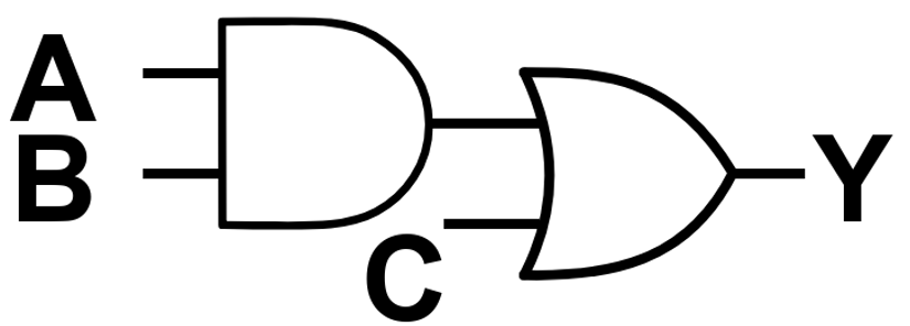
a) Y <= C or (A and B);
b) Y <= C or2 (A and2 B)
c) Y <= C + (A / B)
d) Y <= A or (B and C)
View Answer
Explanation: The keyword for AND operation is ‘and’ and the keyword for OR operation is ‘or’. In the circuit above A and B are ANDed and the result of that is ORed with C.
8. Write the VHDL statements for the below logic circuit assuming that each gate has a propagation delay of 10 ns.
a) C <= A and B after 5 ns; Y <= C or D after 5 ns;
b) D <= A and B after 10 ns; Y <= C or D after 10 ns;
c) Y <= C or (A and B);
d) Y <= C or (A and B) after 10 ns;
View Answer
Explanation: The keyword for AND operation is ‘and’ and the keyword for OR operation is ‘or’. In the circuit above A and B are ANDed and the result of that operation, D, is ORed with C.
The keyword ‘after’ is used to model the propagation delay. 10 ns stands for 10 nano 10-9 seconds.
9. Identify the Boolean expression that results from the following VHDL code.
D <= A or B;
Y <= D nand C;
a) Y = ((A + B).C)’
b) Y = (A+B).C
c) Y = A+ (B.C)
d) Y = A.(B +C)
View Answer
Explanation: The keyword for NAND operation is ‘nand’ and the keyword for OR operation is ‘or’. In the circuit above A and B are ORed and the result of that operation, D, is NANDed with C.
D = A + B.
Y = (D.C)’
So, we get the result as ((A + B).C)’
Sanfoundry Global Education & Learning Series – Logic Design.
To practice all areas of Logic Design, here is complete set of 1000+ Multiple Choice Questions and Answers.
If you find a mistake in question / option / answer, kindly take a screenshot and email to [email protected]
