This set of Nanotechnology Multiple Choice Questions & Answers (MCQs) focuses on “Structural Analysis – STM”.
1. Who were the inventers of scanning tunneling microscope?
a) C.V Raman and Pearl Kendrick
b) Antonie Van Leewenhoek and Aaron Klug
c) Heirich Rohrer and Gerd binning
d) Robert Boyle and Zhang Heng
View Answer
Explanation: Scanning tunneling microscope is an instrument used for imaging surfaces at the atomic level. It was invented by Gerd Binning and Heirech Rohrer in 1981. They worked at IBM Zürich then and had received a Nobel prize in physics in 1986 for their invention.
2. What is the principle behind scanning tunneling microscope?
a) Mass – energy equivalence
b) Quantum tunneling
c) Special relativity
d) Kinetic molecular theory
View Answer
Explanation: Scanning tunneling microscope is based on the concept of quantum tunneling. It’s a phenomenon in which a wave function can propagate through a potential barrier. The tip of the microscope is brought very close to the surface for examination. A bias voltage is applied between the two which allows electrons to tunnel through the vacuum separating them.
3. Which of these statements best matches the description of scanning tunneling spectroscopy?
a) Tip of microscope is in a constant position above the surface
b) The bias voltage is kept constant
c) The technique is always carried out in low magnetic fields
d) No reconstruction of local density of the electronic states
View Answer
Explanation: In scanning tunneling spectroscopy, the tip of the microscope is kept in a constant position above the surface. The bias voltage is varied while the resultant change in current is recorded. The local density of the electronic states can be reconstructed using high magnetic fields and in the presence of impurities.
4. Which of the following is not a drawback of the scanning tunneling microscopy?
a) Clean and stable surface
b) Sharp tips
c) Complicated electronics
d) High resolution
View Answer
Explanation: Scanning tunneling microscope has a list of drawbacks such as the requirement of stable and clean sample surfaces which is close to impossible. It is compatible only with conductive surfaces such as metals and semiconductors. It is a quite expensive instrument especially UHV version that makes use of sophisticated electronics.
5. Pick the odd one out.
a) Lateral scanner
b) RHEED gun
c) Tungsten scanning tip
d) Vibration isolation system
View Answer
Explanation: The components found in a scanning tunneling microscope are lateral scanner, scanning tip, piezoelectrically controlled height and coarse sample to sample approach mechanism. The microscope has a vibration isolation system that is packed with dedicated electronics and a computer.
6. What is the material used for constructing the scanner tube?
a) Silicon carbide ceramic composites
b) Aluminium nitride ceramic
c) Lead zirconate titanate ceramic
d) Zirconium oxide – alumina ceramic
View Answer
Explanation: In the scanning tunneling microscope, the scanner is a hollow tube of a radially polarized piezoelectric with metallized surfaces. The tube is constructed by a lead zirconate titanate ceramic composite.
7. What has to be done for obtaining usable results in the presence of extremely sensitive tunneling current?
a) Electrical levitation
b) Undamping vibrations with eddy currents
c) Acoustic oscillation
d) Use of gas spring systems
View Answer
Explanation: The extreme sensitivity of the tunneling current can be controlled by proper vibration isolation or a rigid scanning tunneling microscope body to obtain useable results. The very first scanning tunneling microscope made use of magnetic levitation to keep the device free from vibrations. Nowadays, mechanical spring or gas spring systems are employed. Vibration damping mechanisms are also implemented at times.
8. Predict the order of steps followed during viewing a sample under scanning tunneling microscopy.
a) Tip is held close to sample ➔ Application of bias voltage between tip and ample ➔ Tip receives tunneling current ➔ Tip is moved across the surface ➔ Digital images of the surface are formed
b) Digital images of the surface are formed ➔ Tip receives tunneling current ➔ Application of bias voltage between tip and ample ➔ Tip is moved across the surface ➔ Tip is held close to sample
c) Application of bias voltage between tip and ample ➔ Tip is held close to sample ➔ Tip receives tunneling current ➔ Digital images of the surface are formed ➔ Tip is moved across the surface
d) Tip receives tunneling current ➔ Digital images of the surface are formed ➔ Tip is moved across the surface ➔ Tip is held close to sample ➔ Application of bias voltage between tip and ample
View Answer
Explanation: For imaging the sample, the tip of the microscope is brought close to it by a cross positioning mechanism that is usually monitored visually. The tip positioning is controlled by piezoelectric scanner tubes. A bias voltage is applied between the sample and the tip which starts receiving the tunneling current. Once this is achieved the tip is moved across the surface in a discrete x-y matrix. Digital images of the surface are formed during the process.
9. What is the separation kept between the tip and sample while raster scanning of the sample?
a) 4Å -7Å
b) 5Å- 15Å
c) 30Å – 40Å
d) 55Å – 70Å
View Answer
Explanation: The tip and sample separation must be kept around 4-7Å or 0.4-0.7 nm. The range should not fall below 3Å where repulsive interactions are dominant. It should be within 3Å and 10Å since attractive forces become prominent here.
10. Choose the correct statement from the following with respect to constant current mode.
a) Very fast mode of sample scanning
b) Feedback electronics adjust height by a voltage
c) Height of the scanner remains unchanged irrespective of the sample topography
d) Image scanned has only electron density data
View Answer
Explanation: The scanner height in a scanning tunneling microscope, operating in constant current mode, can be adjusted by applying voltage to piezoelectric height control mechanism system. It is a relatively slow method for scanning the sample. Scanner height has to be changed according to the sample topography. When the surface is flat, voltage applied to the z-scanner will reflect variations in local charge density. However, due to atomic step the height of the scanner has to be changed. Image scanned using this instrument contains both topographical and electron density data.
11. Which of the given expressions correctly indicates the exponential decay of the current amplitude with the distance?
a) I = JA
b) I ~ Ve-cd
c) I = √(P/R)
d) I ~ Mdɛ
View Answer
Explanation: The expression that correctly represents the exponential decay of the current amplitude with the distance is given by;
I ~ Ve-cd
Where I is the tunneling current, V is the voltage between probe and sample, c is constant and d is the probe-sample separation distance.
12. Label the given diagram of a scanning tunneling microscope.
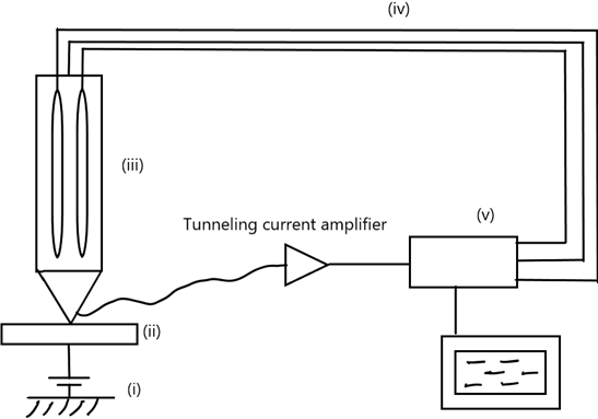
a) i) Control voltages for piezotube; v) Sample
b) ii) Scanner tube; iv) Peizoelectric tube
c) iii) Piezoelectric tube; i) Tunneling voltage
d) v) Distance control and scanning unit; iii) Scanner tip
View Answer
Explanation: In the above given diagram of a scanning tunneling microscope the marked parts are: i) tunneling voltage, ii) sample, iii) piezoelectric tube with electrodes, iv) control voltages for piezotube, v) distance control and scanning unit.
Sanfoundry Global Education & Learning Series – Nanotechnology.
To practice all areas of Nanotechnology, here is complete set of 1000+ Multiple Choice Questions and Answers.
If you find a mistake in question / option / answer, kindly take a screenshot and email to [email protected]
