This set of Nanotechnology Multiple Choice Questions & Answers (MCQs) focuses on “Structural Analysis – AFM”.
1. Who invented Atomic Force Microscope?
a) Gerd Binning and Calvin Quate
b) Ernst Ruska and Klaus Von Klitzing
c) Heinrich Rohrer and Hans Daucher
d) Wolfgang Ebert and Felix Bloch
View Answer
Explanation: The Atomic Force Microscope (AFM) was invented by IBM scientists in 1985, by Gerd Binning. It had its first experimental impression made in 1986 by Gerber, Calvin Quate and Gerd Binning. The AFM was first commercially available in 1989.
2. What is the major difference between AFM and optical microscopy?
a) Maintenance
b) Beam irradiation
c) Resolution
d) Cost of the device
View Answer
Explanation: The major differences between atomic force microscopy and technologies such as optical microscopy and electron microscopy is that AFM doesn’t make use of lenses or beam irradiation. Hence, it doesn’t suffer from a limitation in spatial resolution due to diffraction and aberration.
3. Which of the following is not an application of atomic force microscopy in solid state physics?
a) Study changes in physical properties
b) Identifying atoms at the surface
c) Evaluation of interactions between a specific atom and neighboring atoms
d) Image microtubules and measure their stiffness
View Answer
Explanation: Atomic force microscopes are used in solid state physics for identifying atoms on the sample surface. They can also be employed to study changes in the physical properties that develop due to changes in atomic arrangement through atomic manipulation. Another application of AFM includes evaluating interactions between a specific atom and its neighboring atoms.
4. Pick out the odd one out from the following statements regarding atomic force microscopy.
a) Provides a 3D surface profile
b) Does not suffer from charging artifacts in the final image
c) Functions perfectly in a liquid environment
d) Has a maximum scanning area
View Answer
Explanation: The advantages of atomic force microscopy include – i) 3D surface profile of the sample; ii) No requirement for special treatments to irreversibly change or damage the sample; iii) No charging artifacts in the final image; iv) Ability to properly operate in ambient air or even a liquid environment. One of the main downsides to this method is the limited scanning area and height.
5. Label the given diagram of atomic force microscope.
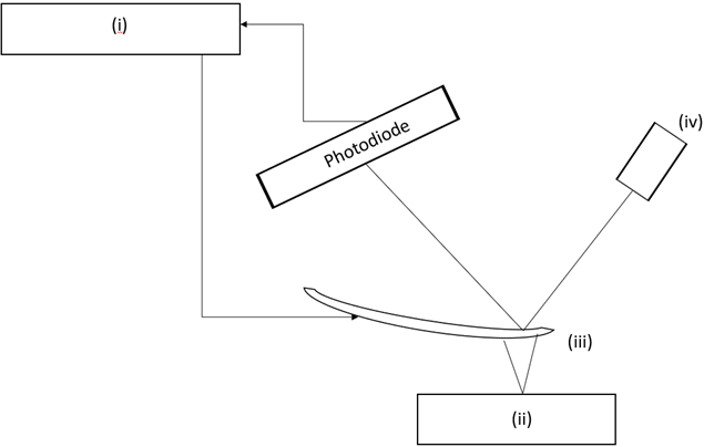
a) i) Laser; ii) Sample
b) iii) Cantilever and tip; iv) Detector
c) i) Feedback electronics; ii) Sample
d) iii) Detector; iv) Laser and cantilever
View Answer
Explanation: The correct labelling’s for the atomic force microscope diagram is; i) Detector and feedback electronics; ii) Sample; iii) Cantilever and tip; iv) Laser. AFM is able to produce images upon scanning the sample surface using a small cantilever, whose height can be adjusted.
6. Which of these is not a major ability of atomic force microscopy?
a) Topographic imaging
b) Pressure measurement
c) Force measurement
d) Manipulation
View Answer
Explanation: Atomic force microscopy is known to have 3 major abilities – force measurement, topographic imaging, manipulation. In force measurement, AFMs can be used to measure the forces between the probe and the sample as a function of their mutual separation. In case of topographic imaging, 3D imaging of the topography of the sample surface is carried out at a high resolution. For manipulation, the forces between the tip and sample are used to change the properties of the sample in a controlled way.
Sanfoundry Global Education & Learning Series – Nanotechnology.
To practice all areas of Nanotechnology, here is complete set of 1000+ Multiple Choice Questions and Answers.
If you find a mistake in question / option / answer, kindly take a screenshot and email to [email protected]
