This set of Nanotechnology Multiple Choice Questions & Answers (MCQs) focuses on “Nano Structured Semiconductor Materials”.
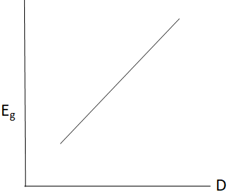
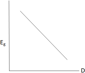
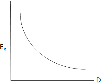
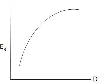
1. Which of the following graph depicts the variation of energy gap with the particle size?
a)
b)
c)
d)
View Answer
Explanation: When the sizes of the particles are reduced to nano-scale, quantum confinement comes into the picture and as a result energy band gap increases. Quantum confinement is the restriction on the motion of the carriers (electrons and holes) in one or more directions by the potential barriers. So, the electron hole pairs are now closer to each other and Coulombic interaction between them cannot be neglected. This gives rise to an overall higher kinetic energy.
2. What is an exciton in a semiconductor?
a) Electron-Electron pair
b) Electron-Hole pair
c) Electron-Phonon pair
d) Hole-Hole pair
View Answer
Explanation: Exciton is an electron-hole pair. It is formed when an electron in the valence band gets raised to conduction band by absorbing sufficient amount of energy needed to overcome this band gap, leaving behind a hole. The exciton is a quasi-particle with no electrical charge on it.
3. Luminescence is created when electrons possessing high amount of energy strike against a semiconductor material–This is the principal of which kind of luminescence?
a) Cathodoluminescence
b) Photoluminescence
c) Electroluminescence
d) Thermoluminescence
View Answer
Explanation: Cathodoluminescence occurs when highly energetic electrons are incident on a luminescent material, thereby causing emission of photons. It is considered to be the reverse process of photo electric effect.
4. How does Silicon behave at 0K?
a) Conductor
b) Super conductor
c) Semiconductor
d) Insulator
View Answer
Explanation: Semiconductors at 0K start behaving the same way as insulators. It has a filled valence band separated from an empty conduction band, by a huge band gap constituting the forbidden region where no electron exists.
5. The lifetime of fluorescence is longer than phosphorescence.
a) True
b) False
View Answer
Explanation: The process of fluorescence has an average lifetime of 10-10 to 10-7 seconds, while the average lifetime of phosphorescence ranges between 10-5 and 10+3 seconds.
6. Where do the impurity states get formed in an n-type and p-type doped semiconductor?
a) Below the bottom of the conduction band and just above the top of the valence band respectively
b) Below the top of the valence band and just above the bottom of the conduction band respectively
c) Just above the bottom of the conduction band and just below the top of the valence band respectively
d) Just above the top of the valence band and just below the bottom of the conduction band respectively
View Answer
Explanation: Impurities are formed just below the bottom of the conduction band and just above the top of the valence band in an n-type and p-type doped semiconductor respectively. Since, there is a close proximity of these impurity states to their respective energy bands, a high probability of excitation of extrinsic carriers to these bands exists. This increases the electrical conductivity of doped semi-conductor.
7. Which of the following is not a phonon?
a) Optical
b) Longitudinal
c) Acoustic
d) Leptons
View Answer
Explanation: Leptons are building blocks of matter. They are elementary particles which are charged and have a distinct mass. Acoustic and Optical phonons are two major types of phonons exhibited by unit cell. Longitudinal and transverse acoustic phonons are two forms of acoustic phonons that are often abbreviated as LA and TA.
8. Which of the following statement is correct regarding p-n junction?
a) At equilibrium, there is no movement of electrons and holes across the p-n junction
b) On applying voltage, only electrons move across the junction
c) Bias condition for current injection is known as reverse bias
d) On applying voltage, only holes move across the junction
View Answer
Explanation: At equilibrium, there is no movement of electrons and holes across the p-n junction but on applying voltage, both the electrons and holes move across the junction. The bias condition for current injection is forward bias.
9. What are phonons?
a) Sub-atomic particles
b) Quasi-particle
c) Quantum of electromagnetic radiation
d) Atoms and molecules
View Answer
Explanation: Quasi-particles are elementary excitations in solids. Phonons are elementary vibrations in condensed matter, and hence it is often referred to as quasi-particles.
10. Which of the following is not a requirement for an ideal semiconductor nanostructure?
a) Density
b) Uniformity
c) Low melting point
d) Confinement potential
View Answer
Explanation: An ideal semiconductor nanostructure should have uniform shape, size, and composition. Dense nanostructures have many applications. Potential wells confining electrons and holes should be sufficiently deep to prevent the thermal excitation of these carriers out of the nanostructures.
11. Which of the following is not an application of semiconductor nano-crystals?
a) Food colouring
b) LEDs
c) Ultrasensitive detection
d) Cellular imaging
View Answer
Explanation: Semiconductor nano crystals are being used in LEDs. They have also found their way into cellular imaging and ultrasensitive detection. However, they have not been used in food colouring yet.
More MCQs on Nano Structured Material:
- Nano Structured Material MCQ (Set 2)
- Nano Structured Material MCQ (Set 3)
- Nano Structured Material MCQ (Set 4)
Sanfoundry Global Education & Learning Series – Nanotechnology.
To practice all areas of Nanotechnology, here is complete set of 1000+ Multiple Choice Questions and Answers.
If you find a mistake in question / option / answer, kindly take a screenshot and email to [email protected]
