This set of Microelectronics Multiple Choice Questions & Answers (MCQs) focuses on “MOS Amplifiers – Common Source Stage”.
1. What is the voltage gain of the following circuit? Neglect channel length modulation.
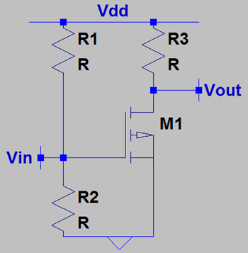
a) -gm*R3
b) -gm*R2
c) -gm*R1
d) -gm*R3*(R1||R2)
View Answer
Explanation: The above circuit shows a Common Source stage biased by the voltage divider biasing method. The biasing circuit doesn’t affect the voltage gain-it only helps us to establish a suitable bias point. The voltage gain is simply -gm*R3.
2. What is the input resistance of the following circuit? Neglect Channel Length Modulation.
a) R1||R3
b) R1||R2
c) R1||R2||R3
d) Infinite
View Answer
Explanation: The biasing circuit impedes the input signal with an input resistance of R1||R2. This implies that the input to the MOSFET is VIN – IG(R1 || R2), note that IG is almost negligible.
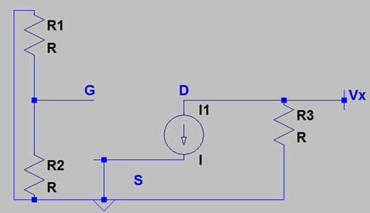
3. What is the output resistance of the following circuit? Neglect Channel Length Modulation.
a) 0
b) R3 || R1
c) R3 || R2
d) R3
View Answer
Explanation: The output resistance for the above circuit is R3. This can be calculated by turning all independent voltage sources off and we place a small voltage source at the output and measure the current. We need to use the small signal model of the MOSFET and the circuit becomes as shown below. Now, we note that I1 is 0 since I1=ƒ(VGS) and VGS=0. Hence, VX/IX = R3.
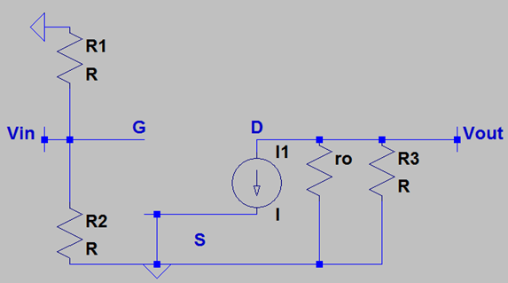
4. In presence of Channel length modulation, what is the voltage gain of the following circuit?
a) -gm*(R3-ro)
b) -gm*R3
c) -gm*(R3+ro)
d) -gm*(R3||ro)
View Answer
Explanation: We will have to draw the small signal model of the MOSFET and turn all independent voltage sources off to solve the circuit. Next we apply an input voltage at the gate and note that VG is almost equal to VIN since the gate current is negligible. At the drain side, we find that I1 flows through the parallel combination of ro & R3. Thus, the output voltage is gm*VIN*(ro||R3) & the voltage gain becomes gm*(ro||R3).
5. In presence of Channel Length Modulation, what is the input resistance of the following circuit?
a) R1||R3
b) R1||R2
c) R1||R2||R3
d) Infinite
View Answer
Explanation: Channel Length modulation won’t affect the internal resistance as it affect the drain side only. The internal resistance is still R1||R2.
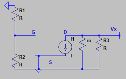
6. What is the output resistance of the following circuit? Neglect Channel Length Modulation.
a) R3 || R1 ||ro
b) R3 || ro
c) R3 || R2
d) 0
View Answer
Explanation: The output resistance is calculated using the small signal model and turning all independent voltage sources off. Note that R1 & R2 doesn’t affect the output since the gate isolates it. Henceforth, we find that ro & R3 are simply parallel to each other which makes the output resistance R3 || ro.
7. In presence of channel length modulation, what is the voltage gain of the circuit?
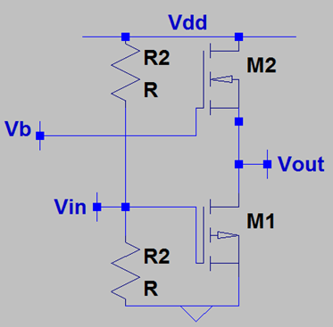
a) -gm1*(ro1+ro3)
b) -gm3*(ro1-ro3)
c) -gm1*(ro1||ro3)
d) Error
View Answer
Explanation: To find the small signal gain, we draw the small signal model of both the MOSFETs and turn off all independent voltage source. Now we apply a voltage at the gate of M1 & find that I1 flows through the parallel combination of ro1 and ro2. Note that I2 is 0 since VB is turned off. Hence, the output voltage is gm*VIN*(ro1||ro2) and the overall voltage gain becomes gm*(ro1||ro2).
8. In presence of channel length modulation, what is the input resistance of the circuit?
a) (R1+R2)
b) (R1||R2)
c) R1
d) R2
View Answer
Explanation: The input resistance of the circuit is calculated from VIN and we note that the channel length modulation is present in the output side. So the input resistance is equal to
R1||R2.
9. In presence of channel length modulation, what is the input resistance of the circuit?
a) (ro1||ro3)
b) (ro1+ro3)
c) ro3
d) ro1
View Answer
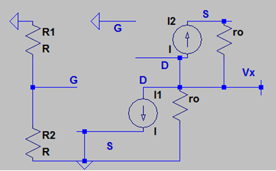
Explanation: The output resistance is to be calculated by turning off all the independent voltage source and place a voltage source at the output. Note that both I1 & I2 becomes 0 and we only have ro1 and ro2 left. The overall output resistance is (ro1||ro3). We must remember that ro1 are ro3 not physical resistors. They will manifest themselves when the circuit is on and their values will be set by the value of I1 & I2 respectively. We have only calculated what are the possible impedances at the output side at low frequency.
10. What happens to the voltage gain of the following circuit if the aspect ratio is increased by a factor of 2 but the overdrive voltage is kept constant?
a) It increases by a factor of 2
b) It decreases by a factor of 2
c) It increases by a factor of √2
d) It decreases by a factor of √2
View Answer
Explanation: The voltage gain of the circuit was found to be gm*R3. We note that gm is proportional to the aspect ratio if the overdrive voltage is kept constant. Hence, the voltage gain will increase proportionately by a factor of 2.
11. What happens to the voltage gain of the following circuit if the aspect ratio is increased by a factor of 2 but the drain current is kept constant?
a) It increases by a factor of 4
b) It decreases by a factor of 4
c) It increases by a factor of √2
d) It decreases by a factor of √2
View Answer
Explanation: The voltage gain of the circuit was found to be gm*R3. We note that gm is proportional to the square root of the aspect ratio if the drain current is kept constant. Hence, the voltage gain will increase proportionately by a factor of √2.
Sanfoundry Global Education & Learning Series – Microelectronics.
To practice all areas of Microelectronics, here is complete set of 1000+ Multiple Choice Questions and Answers.
If you find a mistake in question / option / answer, kindly take a screenshot and email to [email protected]
