This set of Microelectronics Multiple Choice Questions & Answers (MCQs) focuses on “MOS Cascode”.
1. The Cascode Stage is a Cascade of ______________
a) CS & CD stage
b) CG & CD stage
c) CS & CG stage
d) Driver and follower stage
View Answer
Explanation: The Cascode stage is a cascade of a CS & CG stage. The input is applied to the CS stage while the CG stage behaves more like a current source. The other cascaded stages aren’t referred to as Cascode stages.
2. Which MOSFET is behaving as the degenerating device?

a) M1
b) M2
c) Neither of the MOSFETs
d) Both the MOSFETs
View Answer
Explanation: M2 degenerates the output impedance of M2. This output impedance is seen from the drain terminal.
3. Which MOSFET is behaving as the Cascode device?
a) M1
b) M2
c) Neither of the MOSFETs
d) Both the MOSFETs
View Answer
Explanation: M2 is behaving as the Cascode device. It is being used as a current source to increase the output impedance of M1.
4. In absence of M2, what is the minimum output voltage swing in the following circuit?
a) One overdrive voltage
b) Twice the overdrive voltage
c) Thrice the overdrive voltage
d) Four times the overdrive voltage
View Answer
Explanation: In absence of M1, the minimum voltage swing can be one overdrive voltage. This is because the input voltage has to be less than the output voltage by the threshold voltage. Hence, the output voltage faces a restriction of one overdrive voltage.
5. In absence of M2, what is the minimum output voltage swing in the following circuit?
a) One overdrive voltage
b) Twice the overdrive voltage
c) Thrice the overdrive voltage
d) Four times the overdrive voltage
View Answer
Explanation: Firstly, the output voltage provides an amplified version of the input voltage at saturation. If the MOSFET has to operate in the saturation region, the drain voltage i.e. the output voltage has to more than the gate voltage by the threshold voltage. We have two MOSFETs and hence, the drain voltage of M2 has to be greater than its VGS2 by one threshold voltage. Now, VS2=VD1 and VD1 itself has to be more than its VGS1 i.e. the input voltage by one threshold voltage. Hence, the minimum output voltage swing becomes two threshold voltage.
6. What is the output resistance at node B if both the MOSFETs suffer from channel length modulation?

a) (ro1||1/gm2||ro2)
b) (R3+ro2)/(1+(gm2*ro2)
c) (R3+ro2)/(1+(gm2*ro2)||ro1
d) (ro1||1/gm2||ro3)
View Answer
Explanation: Two branches are present at node B. One connect to the source of M2 which offers an impedance of (R3+ro2)/(1+(gm2*ro2)). The other connects to the drain of M1 which offers an impedance of ro1. Hence, if we measure the output impedance at B, we follow the procedure of Thevenin and find that these two impedances will be in parallel to each other. The overall impedance becomes (R3+ro2)/(1+(gm2*ro2)||ro1.
7. What is the output resistance at node B if both the MOSFETs suffer from channel length modulation and M2 suffers from Body Effect?
a) (R3+ro1)/(1+(gm2-gmb2)*ro1)||ro2
b) (R1+ro2)/(1+(gmb2*ro2))||ro1
c) (R2+ro2)/(1+(gm2+gmb2)*ro2)||ro1
d) (R3+ro2)/(1+(gm2+gmb2)*ro2)||ro1
View Answer
Explanation: Two branches are present at node B. One connect to the source of M2 which offers an impedance of (R3+ro2)/(1+(gm2+gmb2)*ro2). The other connects to the drain of M1 which offers an impedance of ro1. Hence, if we measure the output impedance at B, we follow the procedure of Thevenin and find that these two impedances will be in parallel to each other. The overall impedance becomes (R3+ro2)/(1+(gm2+gmb2)*ro2)||ro1.
8. What is the output resistance at node A if both the MOSFETs suffer from channel length modulation?
a) R3||[1+(gm2+gmb2)*ro2]*ro1+ro2
b) R3||[1+gm1*ro2]*ro2+ro1
c) [1+gm2*ro1]*ro1+ro2
d) R3||[1+(gmb2*ro2)]*ro1+ro1
View Answer
Explanation: The output impedance at node A will be R3 in parallel to the output impedance looking into the drain of M2. M2 is degenerated by M1 and the impedance looking into its drain terminal becomes [1+gm2*ro2]*ro1+ro2. The overall resistance is R3||[1+gm2*ro2]*ro1+ro2.
9. What is the output resistance at node A if both the MOSFETs suffer from channel length modulation?
a) R3||[1+gm2*ro2]*ro1+ro2
b) R3||[1+gm1*ro2]*ro2+ro1
c) [1+gm2*ro1]*ro1+ro2
d) R3||[1+(gm1+gmb2)*ro1]*ro2+ro1
View Answer
Explanation: The output impedance at node A will be R3 in parallel to the output impedance looking into the drain of M2. M2 is degenerated by M1 and the impedance looking into its drain terminal becomes [1+(gm1+gmb2)*ro2]*ro1+ro2. The overall resistance is R3||[1+(gm1+gmb2)*ro2]*ro1+ro2.
10. What is the ratio of Voltage at node A to the input voltage in the Cascode stage?
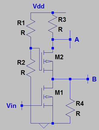
a) -gm2*(R3||ro2||(R3+ro2)/(1+(gmb2*ro2))
b) -gm1*(R4||ro1||(R3+ro2)/(1+(gm*ro2))
c) -gm1*(R3||ro2||(R1+ro2)/(1+(gmb2*ro2))
d) -gm2*(R4||ro1||(R1+ro2)/(1+(gmb2*ro2))
View Answer
Explanation: The ratio of the voltage at node B to the input voltage is the voltage gain of M1 being used as a CS stage. Hence, we can perform a small signal analysis and observe that the voltage gain is -gm1*the total impedance connected to its drain. This will be the output impedance at the node B. Node B has 3 branches. One branch connects to the source of M2 which offers an impedance of (R1+ro2)/(1+(gmb2*ro2) while another branch connects to the drain of M1 which offers a resistance of ro1. Finally, the last branch connects to R4 & all these resistances come in parallel. The overall output impedance is (R4||ro1||(R1+ro2)/(1+(gmb2*ro2)) and the voltage gain becomes -gm1*(R4||ro1||(R1+ro2)/(1+(gmb2*ro2)). Note that we can also calculate the voltage gain if M2 suffers from Body effect.
Sanfoundry Global Education & Learning Series – Microelectronics.
To practice all areas of Microelectronics, here is complete set of 1000+ Multiple Choice Questions and Answers.
If you find a mistake in question / option / answer, kindly take a screenshot and email to [email protected]
