This set of Microelectronics Multiple Choice Questions & Answers (MCQs) focuses on “MOS Amplifiers – Common Gate Stage – Set 2”.
1. In presence of channel length modulation in M1, what is the voltage gain of the following circuit?
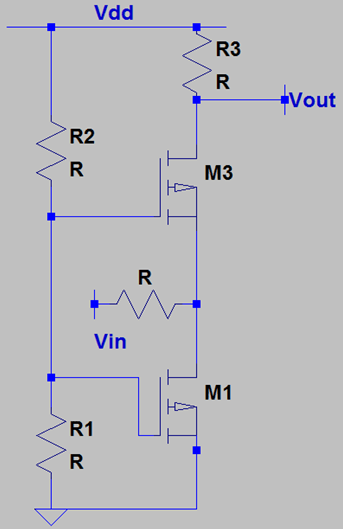
a) \(\{ \frac { (\frac {1}{g_{m3}}||r_{o3}+r_{o1})}{((\frac {1}{g_{m3}}||r_{o3}+r_{o1})+R) } \}\)*(gm3*R3)
b) \(\{ \frac { (\frac {1}{g_{m3}}||r_{o3}||r_{o1})}{((\frac {1}{g_{m3}}||r_{o3}||r_{o1})+R) } \}\)*(gm3*R3)
c) \(\{ \frac { (\frac {1}{g_{m3}}||r_{o1})}{((\frac {1}{g_{m3}}||r_{o1})+R) } \}\)*(gm3*R3)
d) \(\frac { \{ (\frac {1}{g_{m3}}||r_{o3}||r_{o1})}{((\frac {1}{g_{m3}}+r_{o3}+r_{o1})+R) \} }\)*(gm3*R3)
View Answer
Explanation: M1 offers an output impedance of ro1 at the drain terminal while M3 offers an output impedance of 1/gm3 at the source terminal. Hence, the input to the source of M3 is a result of voltage division between R and (1/gm3||ro1) and R – the input voltage becomes VIN*(1/gm3||ro1)/((1/gm3||ro1)+R). This voltage will get multiplied by a factor of gm3*R3 due to the CG stage and we get the overall voltage gain as \(\{ \frac { (\frac {1}{g_{m3}}||r_{o1})}{((\frac {1}{g_{m3}}||r_{o1})+R) } \}\)*(gm3*R3).
2. In presence of Body effect and Channel Length Modulation in M3 and only channel length modulation in M1, what is the voltage gain of the following circuit?
a) \(\frac { \{ (g_{mb}+ g_m)*r_o + 1 \}R_D}{(r_o + (g_{mb}+ g_m)*r_oR_S + R_S + R_D)}\)
b) \(\frac {(g_{mb}+ g_m)*r_o + 1 \}R_D}{R_D}\)
c) \(\frac {(g_{mb}+ g_m)*r_o + 1 \}R_D}{(r_o + 2R_D)}\)
d) \(\frac { \{ (g_{mb3}+ g_{m3})*r_{o3} + 1 \} R_3}{(r_o + (g_{mb3}+ g_{m3})*r_{o3}(R||r_{o1}) + (R||r_{o1}) + R_3)}\)
View Answer
Explanation: M1 offers an output impedance of ro1 at the drain terminal while M3 offers an output impedance of 1/gm3 at the source terminal. Hence, the input to the source of M3 is a result of voltage division between R and (1/gm3||ro1) and R – the input voltage becomes VIN*(1/gm3||ro1)/((1/gm3||ro1)+R). The total resistance connected to the source terminal is R||ro1. We can calculate the voltage gain of a CG stage with a source resistance, say RS, which comes out to be \(\frac { \{ (g_{mb}+ g_m)*r_o + 1 \}R_D}{(r_o + (g_{mb}+ g_m)*r_oR_S + R_S + R_D)}\). We replace RS by R||ro1 and voltage gain of the following circuit becomes \(\frac { \{ (g_{mb}+ g_{m})*r_{o} + 1 \} R_D}{(r_o + (g_{mb}+ g_{m})*r_{o}(R||r_{o1}) + (R||r_{o1}) + R_D)}\).
3. Will body effect manifest itself in M1?
a) YES
b) NO
c) It may, depending upon VDD
d) It may, depending upon VIN
View Answer
Explanation: For body effect to manifest itself, the source voltage must change with respect to the substrate voltage. For M1, the source voltage doesn’t change since it is connected to the ground and body effect won’t occur in M3.
4. In presence of Body effect and Channel Length Modulation in M3, what is the voltage gain of the following circuit?
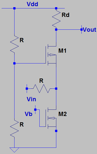
a) Error
b) (1/gm2||1/gm1||ro1)/((1/gm2||1/gm1||ro1)+R)*{(gmb+gm)*ro+1}Rd/(ro1+(gmb+gm)*ro*(R||1/gm2)+(R||1/gm2)+Rd)
c) (1/gm2+1/gm1+ro1)/((1/gm2+1/gm1+ro1)+R)*{(gmb+gm)*ro+1}RD/(ro1+(gmb+gm)*ro*(R||1/gm2)+(R||1/gm2)+RD)
d) (1/gm2+1/gm1+ro1)/((1/gm2+1/gm1+ro1)+R)*{(gmb+gm)*ro+1}RD/(ro1+(gmb+gm)*ro*(R+1/gm2)+(R+1/gm2)+RD)
View Answer
Explanation: M2 offers an output impedance of 1/gm2 at the drain terminal while M1 offers an output impedance of 1/gm1||ro1 at the source terminal. Hence, the input to the source of M3 is a result of voltage division between R and (1/gm2||1/gm1||ro1) and R – the input voltage becomes VIN*(1/gm2||1/gm1||ro1)/((1/gm2||1/gm1||ro1)+R). The total resistance connected to the source terminal is R||1/gm2. We can calculate the voltage gain of a CG stage with a source resistance, say RS, which comes out to be \(\frac { \{ (g_{mb}+ g_m)*r_o + 1 \}R_d}{(r_o + (g _{mb}+ g_m)*r_oR_S + R_S + R_d)}\). Hence, the output voltage for only the CG stage becomes VS*{(gmb+gm)*ro+1}RD/(ro+(gmb+gm)*ro*(R||1/gm2||ro2)+(R||1/gm2||ro2)+RD). The overall voltage gain is (1/gm2||1/gm1||ro1)/((1/gm2||1/gm1||ro1)+R)*{(gmb+gm)*ro+1}RD/(ro1+(gmb+gm)*ro*(R||1/gm2)+(R||1/gm2)+RD). Note that performing a small signal analysis will reveal to the same expression of voltage gain, but it becomes more complicated.
5. In presence of Body effect and Channel Length Modulation in M3 and only Channel Length Modulation in M1, what is the voltage gain of the following circuit?
a) (1/gm2+1/gm1||ro1)/((1/gm2+1/gm1||ro1)+R)*{(gmb+gm)*ro+1}Rd/(ro+(gmb+gm)*ro*(R||1/gm2)+(R||1/gm2)+Rd)
b) 1/gm2+gm2||ro1)/(1/gm2||1/gm1||ro1)*{(gmb+gm)*ro+1}Rd/(ro+(gmb+gm)*ro*(R||1/gm2)+(R||1/gm2)+Rd)
c) 1/gm1+gm1||ro1)/((1/gm1||1/gm2||ro2)+R)*{(gmb+gm)*ro+1}Rd/(ro+(gmb+gm)*ro*(R||1/gm2)+(R||1/gm2)+Rd)
d) (1/gm2||ro2||1/gm1||ro1)/((1/gm2||ro2||1/gm1||ro1)+R)*{(gmb+gm)*ro+1}Rd/(ro+(gmb+gm)*ro*(R||1/gm2||ro2)+(R||1/gm2||ro2)+Rd)
View Answer
Explanation: M2 offers an output impedance of 1/gm2||ro2 at the drain terminal while M1 offers an output impedance of 1/gm1||ro1 at the source terminal. Hence, the input to the source of M3 is a result of voltage division between R and (1/gm2||ro2||1/gm1||ro1) and R – the input voltage becomes VIN*(1/gm2||ro2||1/gm1||ro1)/((1/gm2||ro2||1/gm1||ro1)+R). The total resistance connected to the source terminal is R||1/gm2ro2||. We can calculate the voltage gain of a CG stage with a source resistance, say RS, which comes out to be \(\frac { \{ (g_{mb}+ g_m)*r_o + 1 \}R_d}{(r_o + (g _{mb}+ g_m)*r_oR_S + R_S + R_d)}\). Hence, the output voltage for only the CG stage becomes VS*{(gmb+ gm)*ro+1}Rd/(ro1+(gmb+ gm)*ro*(R||1/gm2||ro2)+(R||1/gm2||ro2)+Rd). The overall voltage gain is (1/gm2||ro2||1/gm1||ro1)/((1/gm2||ro2||1/gm1||ro1)+R)*{(gmb+gm)*ro+1}Rd/(ro+(gmb+gm)*ro*(R||1/gm2||ro2)+(R||1/gm2||ro2)+Rd). If body effect is also present in M2, the calculation is same and only the output resistance of M2 changes.
6. What is the output impedance of the following circuit if only M1 suffers from channel length modulation but M2 doesn’t suffer from any second order effect?
a) Rd||{(1-gm1*ro1)*(R||gm2)+ro1}
b) Rd||{(1+gm1*ro1)*(R-1/gm2)+ro1}
c) Rd||{(1+gm1*ro1)*(R||1/gm2)+ro1}
d) Rd||{(1+gm1*ro1)*(R+1/gm2)+ro1}
View Answer
Explanation: The output impedance of the following circuit is Rd in parallel to the output resistance of the degenerated M1. M1 is degenerated by the resistance connected to the source of M1. The total resistance connected to the source of M1 is R in parallel to the output resistance of M2, which is 1/gm2, and the total resistance connected to the source of M1 is R||1/gm2. The degenerated resistance of M1 is (1+gm1*ro1)*(R||1/gm2)+ro1 and the overall output resistance becomes Rd||{(1+gm1*ro1)*(R||1/gm2)+ro1}.
7. What is the output impedance of the following circuit if both the MOSFET suffer from channel length modulation and body effect?
a) Rd||{(1+(gm1+gmb1)*ro1)*(R||1/(gmb2+gm2)||ro2)+ro1}
b) Rd||{(1+gmb1*ro1)*(R||1/(gm2)||ro2)+ro1}
c) Rd||{(1+(gm1-gmb1)*ro1)*(R||1/(gmb2+gm2)||ro2)+ro1}
d) Rd||{(1+(gm1)*ro1)*(R||1/(gmb2)||ro2)+ro1}
View Answer
Explanation: The output impedance of the following circuit is Rd in parallel to the output resistance of the degenerated M1. M1 is degenerated by the resistance connected to the source of M1. The total resistance connected to the source of M1 is R in parallel to the output resistance of M2, which is 1/(gmb2+gm2)||ro2, and the total resistance connected to the source of M1 is R||1/(gmb2+gm2)||ro2. The degenerated resistance of M1 is (1+(gm1+gmb1)*ro1)*(R||1/(gmb2+gm2)||ro2)+ro1 and the overall output resistance becomes Rd||{(1+(gm1+gmb1)*ro1)*(R||1/(gmb2+gm2)||ro2)+ro1}.
8. How should we select Vb for M2 to work properly?
a) Always more than 0
b) Always less than 0
c) Equal to 0
d) Cannot be less than 0
View Answer
Explanation: M2 is a PMOS. Depending on the output resistance we need from M2, we choose the magnitude of VB but it will always be less than 0.
9. In presence of channel length modulation and body effect in M1 and early effect in Q1, what is the voltage gain?
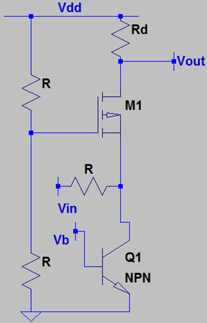
a) (1/gm1||ro1||ro1(Q))/((1/gm1||ro1||ro1(Q))+R)*{(gmb)*ro+1}Rd/(ro+(gmb+gm)*ro*(ro1(Q))+(R+ro1(Q))+Rd)
b) (1/gm1+ro1||ro1(Q))/((1/gm1-ro1||ro1(Q))+R)*{(gm)*ro+1}Rd/(ro+(gmb+gm)*ro*(R||ro1(Q))+(R||ro1(Q))+Rd)
c) (1/gm1||ro1||ro1(Q))/((1/gm1||ro1||ro1(Q))+R)*{(gmb+gm)*ro+1}Rd/(ro+(gmb+gm)*ro*(R||ro1(Q))+(R||ro1(Q))+Rd)
d) Error
View Answer
Explanation: M1 offers an output impedance of 1/gm1||ro1 at the drain terminal while Q1 offers an output impedance of ro1(Q) at the collector terminal. Hence, the input to the source of M3 is a result of voltage division between R and (1/gm1||ro1||ro1(Q)) and R – the input voltage becomes VIN*(1/gm1||ro1||ro1(Q))/((1/gm1||ro1||ro1(Q))+R). The total resistance connected to the source terminal is R||ro1(Q). We can calculate the voltage gain of a CG stage with a source resistance, say RS, which comes out to be \(\frac { \{ (g_{mb}+ g_m)*r_o + 1 \}R_d}{(r_o + (g _{mb}+ g_m)*r_oR_S + R_S + R_d)}\). Hence, the output voltage for only the CG stage becomes VS*{(gmb+gm)*ro+1}Rd/(ro+(gmb+gm)*ro*(R||ro1(Q))+(R||ro1(Q))+Rd). The overall voltage gain is (1/gm1||ro1||ro1(Q))/((1/gm1||ro1||ro1(Q))+R)*{(gmb+gm)*ro+1}Rd/(ro+(gmb+ gm)*ro*(R||ro1(Q))+(R||ro1(Q))+Rd).
10. In presence of channel length modulation in M1 & M3, what is the voltage gain of the following circuit?
a) {(1/gm3||ro3+ro1)/((1/gm3||ro3+ro1)+R)}*(gm3*R3)
b) {(1/gm3||ro3||ro1)/((1/gm3||ro3||ro1)+R)}*(gm3*R3)
c) {(1/gm3||ro3|ro1)/((1/gm3+ro3+ro1)+R)}*(gm3*R3)
d) {(1/gm3+ro3+ro1)/((1/gm3||ro3||ro1)+R)}*(gm3*R3)
View Answer
Explanation: M1 offers an output impedance of ro1 at the drain terminal while M3 offers an output impedance of 1/gm3||ro3 at the source terminal. Hence, the input to the source of M3 is a result of voltage division between R and (1/gm3||ro3||ro1) and R – the input voltage becomes VIN*(1/gm3||ro3||ro1)/((1/gm3||ro3||ro1)+R). This voltage will get multiplied by a factor of gm3*R3 due to the CG stage and we get the overall voltage gain as {(1/gm3||ro3|ro1)/((1/gm3+ro3+ro1)+R)}*(gm3*R3).
Sanfoundry Global Education & Learning Series – Microelectronics.
To practice all areas of Microelectronics, here is complete set of 1000+ Multiple Choice Questions and Answers.
If you find a mistake in question / option / answer, kindly take a screenshot and email to [email protected]
