This set of Microelectronics Multiple Choice Questions & Answers (MCQs) focuses on “Bipolar Current Mirror – Set 2”.
1. In the following circuit, we observe that the base current is not negligible and the current gain is β=8. If the collector current is 4 times the reference current, what should be the base width of Q3 if the base width of Q1 is WB?
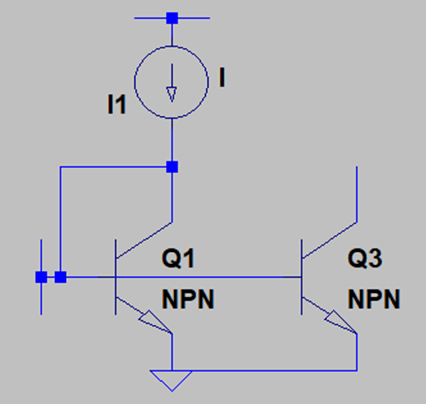
a) 83*WB/9
b) WB/98
c) 24*WB/92
d) WB/9
View Answer
Explanation: We can say that the collector current of Q2 is p*(1/(1+(1/β)*(p+1))) where p is the total no. of transistors connected to Q1. From the given values, we can determine p to be 9. This implies that Q3 is equivalent to 9 identical transistors in parallel and it’s base width is not more than (1/9) times the base width of Q1.
2. In the following circuit, we observe that the base current is not negligible and the current gain is β=64. If the collector current is 8 times the reference current, what should be the area of the emitter of Q3 if the emitter area of Q1 is AE?
a) 35/2*AE
b) 46/9*AE
c) 65/7*AE
d) 74/90*AE
View Answer
Explanation: We can say that the collector current of Q2 is p*(1/(1+(1/β)*(p+1))) where p is the total no. of transistors connected to Q1.From the given values, we can determine p to be 65/7. This implies that Q3 is equivalent to a transistor whose emitter area is not less than 65/7 times the area of the emitter of Q1.
3. The current mirror overcomes all the problems of biasing which came up due to supply rail problems.
a) True
b) False
View Answer
Explanation: The current source, in a current mirror stage, itself proves to be a challenging design. However, the current mirror stage does seem to reduce a lot of problems which came up due to the effect of temperature in a V.D.B. stage. i.e. it does help us to improve the bias design significantly.
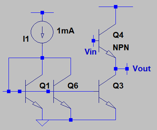
4. In the following circuit, Q3 is biased by a current mirror configuration while Q4 is biased at 1mA. If Q1 & Q6 are identical and only Q3 suffers from early effect, what is ro3 if VA=5V?
a) 1KΩ
b) 40KΩ
c) 10KΩ
d) 30KΩ
View Answer
Explanation: Q3 is biased by a current mirror and we find that the collector current of Q3 is I31/2=0.5mA since the total current due to Q1 and Q6 is equal to the reference current, the base-emitter voltage carries information to generate one-half of the reference current. Hence, ro3=(VA/I3)=10KΩ.
5. In the following circuit, Q3 is biased by a current mirror configuration while Q4 is biased at 1mA. If Q1 & Q6 are identical and only Q3 suffers from early effect, what is the voltage gain if VA=5V?
a) .9974
b) .9746
c) .3658
d) 1
View Answer
Explanation: We note that Q4 is behaving as a follower stage. The transconductance of Q4 is 1/26Ω. The output impedance of Q3 is 10KΩ and thus, the voltage gain becomes .9974.
6. In the following circuit, Q3 is biased by a current mirror configuration while Q4 is biased at 1mA. If Q1 & Q6 are identical and only Q3 suffers from early effect, what is the voltage gain due to the degenerated transconductance of Q4 if VA=5V?
a) .7481
b) .5698
c) .2379
d) .3654
View Answer
Explanation: The transconductance of a degenerated Q4 will be gm0/(1+gm0(ro3||ro4). We have ro4=5KΩ and ro3=10KΩ. Initially, the transconductance of Q4 i.e. gm0 is 1/26Ω. Putting the values, we get the transconductance as .7481.
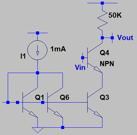
7. In the following circuit, Q3 is biased by a current mirror configuration while Q4 is biased at 1mA. If Q1 & Q6 are identical and only Q3 suffers from early effect, what is the voltage gain due to the degenerated transconductance of Q4 if VA=5V?
a) -3.56
b) -2.56
c) -0.36
d) -3.74
View Answer
Explanation: We note that Q3 generates an output impedance of 10KΩ while the degenerated transconductance of Q4 is 2.9*10-4S. The voltage gain is the voltage gain of a degenerated C.E. stage and it is approximated to \(\frac {–R_C}{((\frac {1}{g_m})+r_{o3})}\) by substituting values we get -3.74.
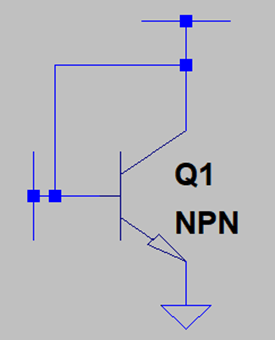
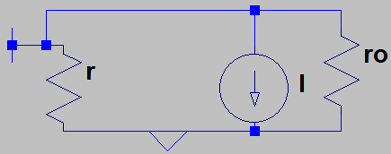
8. What is the impedance of the following circuit, looking into the emitter of the transistor, in presence of early effect?
a) \(\frac {1}{((r_π+r_o) + g_m)}\)
b) \(\frac {1}{(\frac {3}{(r_π-r_o)} + g_m)}\)
c) \(\frac {1}{(\frac {1}{(r_π||r_o)} + g_m)}\)
d) \(\frac {1}{(\frac {2}{(r_o)} + g_m)}\)
View Answer
Explanation: We draw the small signal model and find the Thevenin’s resistance looking into the emitter of Q1. We note that the base and the collector are shorted to AC ground and we write a KCL at the emitter node. Henceforth, the resistance comes out to be \(\frac {1}{(\frac {1}{(r_π||r_o)} + g_m)}\). This is expected because the transistor behaves like a diode-connected transistor in this state ie a two-terminal device.
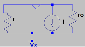
9. What is the impedance looking into the collector of the transistor in presence of early effect? Note that the base is tied to a voltage source.
a) ro
b) 0
c) 3*ro
d) Infinite
View Answer
Explanation: Looking into the collector, the resistance is simply 0. This can be verified from the small signal model but since we are finding the Thevenin’s resistance at the collector node, we note that the base-emitter voltage of the transistor is 0 since both the base & the emitter terminals will be connected to ground. We note that VX gets grounded.
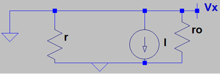
10. What is the input impedance of the following circuit in presence of early effect? Note that the collector is connected to a voltage source.
a) \(\frac {1}{(\frac {1}{(r_π+r_o)} + g_m)}\)
b) \(\frac {1}{(\frac {1}{(r_π-r_o)} + g_m)}\)
c) \(\frac {1}{(\frac {1}{(r_π||r_o)} + g_m)}\)
d) 0
View Answer
Explanation: We draw the small signal model and readily note that the collector is shorted to ground. We conclude that any voltage at the input will get shorted to this ground and the input impedance calculated will be 0.
Sanfoundry Global Education & Learning Series – Microelectronics.
To practice all areas of Microelectronics, here is complete set of 1000+ Multiple Choice Questions and Answers.
If you find a mistake in question / option / answer, kindly take a screenshot and email to [email protected]
