This set of Microelectronics Multiple Choice Questions & Answers (MCQs) focuses on “Linear Operations of OPAMP – Set 2”.
1. What is the -3db pole frequency of the following circuit? Assume that the OPAMP has a finite gain.
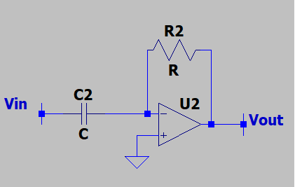
a) (1/G0+1)/R1C1
b) (G0+1)/R1C1
c) (G0)/R1C1
d) (G0-1)/R1C1
View Answer
Explanation: If the OPAMP has a finite gain, the voltage gain is -R1C1s/(1/G0*(1+R1C1s)+1). The 3db pole frequency is where the voltage gain drops approximately to √2 times the original gain. Hence, the pole frequency is (G0+1)/R1C1.
2. If I want to double the gain of the following circuit, what should I do with area of the emitter? Assume that the BJT is ideal but the OPAMP has a finite gain.

a) Double the emitter area
b) Reduce the emitter area by half
c) Multiply the area three times
d) Reduce the emitter area three times
View Answer
Explanation: The voltage gain of the given circuit is [1/(1/G0(R3+(R4+R5))/R3)+(R4+R5)/R3)]*gm*(R5||R4). If we want to double the gain, we may double gm by increasing the emitter area but keeping other parameters constant. Note that as the current double, the collector voltage decreases and this could mean that the transistor may get driven into saturation.
3. What is the voltage gain of the following circuit? Assume that the OPAMP is ideal.

a) –(R3)*(V1/R2+V2)
b) –(R3)*(V1+V2/R1)
c) –(R3)*(V1/R2-V2/R1)
d) –(R3)*(V1/R2+V2/R1)
View Answer
Explanation: This is a simple adder circuit. The voltage gain is given by –(R3)*(V1/R2+V2/R1). Note that this can be derived by applying the superposition theorem- we find the voltage gain for the individual input voltages and finally add the two voltage gains.
4. What is the output voltage of the following circuit? Assume that the OPAMP has a finite voltage gain.
a) {Vin2*R2/(R1+R2)+Vin1*R1/(R1+R2)}*-1/(1/G0(R3+(R1||R2))/R3)+(R1||R2)/R3)
b) {Vin2*R2/(R1+R2)+Vin1*R1/(R1+R2)}*-1/(1/G0(R3+(R1||R2))/R3))
c) {Vin2*R2/(R1+R2)+Vin1*R1/(R1+R2)}*-1/(1/G0(R3+(R1||R2))/R3)-(R1||R2)/R3)
d) {{Vin2*R2/(R1+R2)}*-1/(1/G0(R3+(R1||R2))/R3)+(R1||R2)/R3)
View Answer
Explanation: The OPAMP is literally made to work as an inverting amplifier. With a finite voltage gain, the overall voltage gain becomes -1/(1/G0(R3+(R1||R2))/R3)+(R1||R2)/R3). Moreover, the overall voltage at the input terminal is simply {Vin2*R2/(R1+R2)+Vin1*R1/(R1+R2)}. The output voltage is thus {Vin2*R2/(R1+R2)+Vin1*R1/(R1+R2)}*-1/(1/G0(R3+(R1||R2))/R3)+(R1||R2)/R3).
5. What is the output voltage of the following circuit? Assume that Q1 & Q2 is identical and ideal and the OPAMP is also ideal.

a) gm*(V1+V2)*R2
b) 2*gm*(V1+V2)*R3
c) gm*(V1-V2)*R3
d) gm*(V1+V2)*R3
View Answer
Explanation: The total voltage at the inverting terminal of the OPAMP is -gm*(V1+V2)*(R1||R2). This voltage will simply go to the inverting amplifier and the final output voltage is gm*(V1+V2)*R3.
6. What is the output voltage of the following circuit? Assume that Q1 & Q2 is identical and ideal and the OPAMP has a finite voltage gain.
a) -1/(1/G0(R3+(R1||R2))/R3)-(R1||R2)/R3)*gm*(V1+V2)*(R1||R2)
b) 1/(1/G0(R3+(R1||R2))/R3))*gm*(V1+V2)*(R1||R2)
c) 1/(1/G0(R3+(R1||R2))/R3)+(R1||R2)/R3)*gm*(V1+V2)*(R1||R2)
d) ((R3+(R1||R2))/R3)+(R1||R2)/R3)*gm*(V1+V2)*(R1||R2)
View Answer
Explanation: The total voltage at the inverting terminal of the OPAMP is -gm*(V1+V2)*(R1||R2). The voltage due to the inverting amplifier becomes -1/(1/G0(R3+(R1||R2))/R3)+(R1||R2)/R3), note that the BJT is ideal and does not show early effect. The overall voltage becomes 1/(1/G0(R3+(R1||R2))/R3)+(R1||R2)/R3)*gm*(V1+V2)*(R1||R2).
7. If the two BJT’s are non-identical, what is the voltage gain of the following circuit? Assume that the OPAMP has a finite gain.
a) 1/(1/G0(R3+(R1||R2))/R3))*(gm1*V1+gm1*V2)*(R1||R2)
b) 1/(1/G0(R3+(R1||R2))+(R1||R2)/R3))*(gm1*V1+gm1*V2)*(R1||R2)
c) 1/(1/G0(R3)*(gm1*V1+gm1*V2)*(R1||R2)
d) 1/(1/G0(R3+(R1||R2))/R3)+(R1||R2)/R3))*(gm1*V1+gm2*V2)*(R1||R2)
View Answer
Explanation: The total voltage at the inverting terminal of the OPAMP is –(gm1*V1+gm2*V2)*(R1||R2). The OPAMP shows a finite gain and henceforth, the overall voltage gain becomes The voltage due to the inverting amplifier becomes 1/(1/G0(R3+(R1||R2))/R3)+(R1||R2)/R3))*(gm1*V1+gm1*V2)*(R1||R2).
8. If the two BJT’s are identical but both have early effect, what is the voltage gain of the following circuit? Assume that the OPAMP has a finite gain.
a) gm*(V1+V2)*1/(1/G0(R3+(R1||R2||ro1||ro2))/R3)+(R1||R2||ro1||ro2))/R3)
b) gm*(R1||R2||ro1||ro2)*(R1||R2||ro1||ro2))/R3)
c) gm*(V1+V2)(R1||R2||ro1||ro2)*1/(1/G0(R3+(R1||R2||ro1||ro2))/R3)+(R1||R2||ro1||ro2)/R3)
d) -gm*(V1+V2)(R1||R2||ro1||ro2)*1/(1/G0(R3+(R1||R2||ro1||ro2))/R3)+(R1||R2||ro1||ro2)/R3)
View Answer
Explanation: The total resistance connected to the collector terminal of each transistor is (R1||R2||ro1||ro2), the gain for each stage is simply -gm*(R1||R2||ro1||ro2). The OPAMP, having a finite voltage gain, offers a total output voltage of gm*(V1+V2)(R1||R2||ro1||ro2)*1/(1/G0(R3+(R1||R2||ro1||ro2))/R3)+(R1||R2||ro1||ro2)/R3). Note that ro1=ro2 in this case.
9. If the two MOSFETs are non-identical and has channel length modulation, what is the output voltage of the following circuit if the OPAMP has a finite voltage gain?

a) (gm1*VIN1+gm2*VIN2)*(R1||R2||ro1||ro2)*1/(1/G0(R3+(R1||R2||ro1||ro2))/R3)+(ro1||ro2)/R3)
b) (gm1*VIN1+gm2*VIN2)*(R1||R2||ro1||ro2)*1/(1/G0(R3+(R1||R2||ro1||ro2))/R3)+(R1||R2||ro1||ro2)/R3)
c) (gm1*VIN1+gm2*VIN2)*(R1||R2||ro1||ro2)*1/(1/G0(R3+(R1||R2||ro1))/R3)+(ro1||ro2)/R3)
d) (gm1*VIN1+gm2*VIN2)*(R1||R2|ro2)*1/(1/G0(R3+(R1||R2||ro1||ro2))/R3)+(R1||R2||ro1||ro2))
View Answer
Explanation: The total voltage at the inverting amplifier is –(gm1*VIN1+gm2*VIN2)*(R1||R2||ro1||ro2). This voltage will pass through the inverting amplifier configuration of the OPAMP which has a finite gain and the overall voltage becomes (gm1*VIN1+gm2*VIN2)*(R1||R2||ro1||ro2)*1/(1/G0(R3+(R1||R2||ro1||ro2))/R3)+(R1||R2||ro1||ro2)/R3). Note that ro1 and ro2 are different for each MOSFET.
10. If the two MOSFETs are identical without channel length modulation, by what factor should we change the aspect ratio be changed, so that the output voltage be increased by a factor of 2?
a) Increase by a factor of 2
b) Decrease by a factor of 2
c) Increase by a factor of 4
d) Decrease by a factor of 4
View Answer
Explanation: The output voltage of the following circuit is gm*(V1+V2)(R1||R2||ro1||ro2)*1/(1/G0(R3+(R1||R2||ro1||ro2))/R3)+(R1||R2||ro1||ro2)/R3). This readily shows that if we simply increase the aspect ratio by a factor of 2, the output voltage is also expected to increase by a factor of 2.
Sanfoundry Global Education & Learning Series – Microelectronics.
To practice all areas of Microelectronics, here is complete set of 1000+ Multiple Choice Questions and Answers.
If you find a mistake in question / option / answer, kindly take a screenshot and email to [email protected]
