This set of Microelectronics Multiple Choice Questions & Answers (MCQs) focuses on “MOS Amplifiers – Common Drain Stage”.
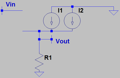
1. What is the voltage gain of the following circuit in absence of any second order effect?
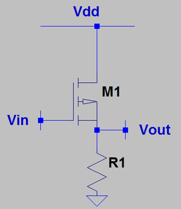
a) R1/(1/gm+R1)
b) R1/(1/gm-R1)
c) R1/(1/gm+2*R1)
d) R1/(1/2*gm+R1)
View Answer
Explanation: We need to draw the small signal model of the MOSFET. Firstly, we note that VGS=VIN-VOUT while VOUT=I*R1. Finally, I is gm*VGS which we can use to represent VGS in terms of VOUT. Finally, we use the first equation and get the voltage gain as R1/(1/gm+R1).
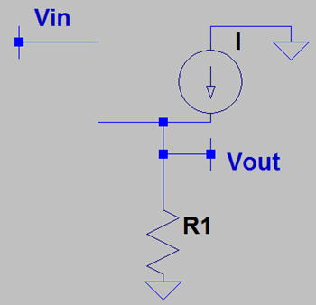
2. What is the voltage gain of the following circuit in presence of body effect?
a) R1/(1/gm+R1)
b) gm*R1/(1+(gm+gmb)*R1)
c) gm*R1/(1+(gm+gmb)*2R1)
d) 1/(1+(gm+gmb)*R1)
View Answer
Explanation: We will draw the small signal model and turn off all independent voltage sources. Next, we apply an input at the gate and note that VGS=VIN-VOUT while VOUT=ID*R1. Next we apply KCL at the source and we can write gm*VGS+gmb*VBS=VOUT/RS. We note that VBS=-VOUT. Now, we can replace VGS & VBS in terms of VIN & VOUT to reach the expression of voltage gain as gm*RS/(1+(gm+gmb)*RS).
3. Can the follower stage give a voltage gain of 1?
a) Yes
b) No
c) If R1 is infinite
d) If R1 is 0
View Answer
Explanation: The follower stage can not give a voltage gain of 1. In absence of second order effects, the expression of voltage gain is R1/(1/gm+R1). We observe that if R1 becomes infinite, the voltage gain becomes gm which is not equal to 1. If R1 is 0, the output voltage becomes 0.
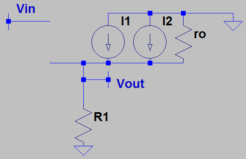
4. In presence only channel length modulation, what is the voltage gain of the following circuit?
a) ro||R1/(1/gm)
b) ro||R1/(2/gm+(ro||R1))
c) ro||R1/(1/gm+(ro||R1))
d) ro||R1/(ro||R1))
View Answer
Explanation: We need to draw the small signal voltage gain of the MOSFET and turn off all independent voltage sources. We readily note that ro and R1 are in parallel to each other. So, I1 flows through ro||R1 and the output voltage is I1*(ro||R1). We note that VIN=VGS+VOUT & I1=gm*VGS. Thereby, we can derive the expression of VOUT/VIN i.e. the voltage gain as ro||RS/(1/gm+(ro||RS)).
5. In presence of body effect and channel length modulation, what is the voltage gain of the following circuit?
a) gm*(ro+R1)/(1+(gm+gmb)(ro+R1))
b) gm*(ro||R1)/(1+(gm+gmb)(ro+R1))
c) gm*(ro+R1)/(1+(gm+gmb)(ro||R1))
d) gm*(ro||R1)/(1+(gm+gmb)(ro||R1))
View Answer
Explanation: We perform a small signal analysis after turning off all independent voltage source. Firstly, we note that ro & R1 are parallel to each other. Hence, the resultant current of the two dependent current sources will flow through the parallel combination of ro & R1 to generate VOUT. Now, we note that VIN=VGS+VOUT and we perform a KCL at the source node where gm*VGS+gmb*VBS=VOUT/R1 and VBS=-VOUT. Finally, we can derive the voltage gain from the input to the output as gm*(ro||R1)/(1+(gm+gmb)(ro||R1)).
6. In presence of channel length modulation, what is the voltage gain of the following circuit?
a) ro||R2/(1/gm+(ro||R2))
b) ro+R2/(1/gm+(ro+R2))
c) ro||R2/(1/gm+(ro+R2))
d) ro+R2/(1/gm+(ro||R2))
View Answer
Explanation: The biasing circuit doesn’t really impact the expression of voltage gain, as a sincere approximation, because the gate offers infinite impedance. Hence, the expression of voltage gain remains unaffected and it is ro||RS/(1/gm+(ro||RS)) which is similar to the voltage gain of a follower stage with channel length modulation. We can perform the small signal analysis again and will return to the same expression.
7. In presence of channel length modulation, what is the voltage gain of the following circuit?

a) ro+R2+R5+R6+R7/(1/gm+(ro+R2+R5+R6+R7))
b) ro||R2||R5||R6||R7/(1/gm+(ro||R2||R5||R6||R7))
c) ro||R2||R5||(R6+R7)/(1/gm+(ro||R2||R5||(R6+R7)))
d) (ro||R2)+(R5||(R6+R7))/(1/gm+(ro||R2)+(R5||(R6+R7))
View Answer
Explanation: We calculate the total resistance connected to the source of M1. This comes out to be R2||R5||R6+R7. In presence of only one resistance RS connected to the source, the expression of voltage gain is ro||RS/(1/gm+(ro||RS)). We only replace RS as R2||R5||R6+R7 and the expression of voltage gain becomes ro||R2||R5||(R6+R7)/(1/gm+(ro||R2||R5||(R6+R7))).
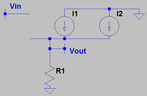
8. In presence of only body effect, what is the output resistance of the following circuit?
a) 1/(gm)
b) 1/(gmb)
c) 1/(gm+gmb)
d) 1/(gm-gmb)
View Answer
Explanation: We draw the small signal model and turn off all independent sources. We note that I1=gm*VGS & I2=gmb*VBS. Noting that VBS=-VOUT, we can represent the dependent current source for I2 as a resistor having a value of 1/gmb while I1 is represented as 1/gm. Henceforth, we note that these two resistances are in parallel and are connected to the source. We observe that R2 is also connected to the source and comes in parallel to 1/(gm+gmb) since they are connected from the source to the ground. The output resistance comes out to be (1/gm||1/gmb)||R2 i.e. 1/(gm+gmb)||R2.
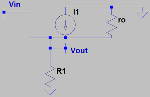
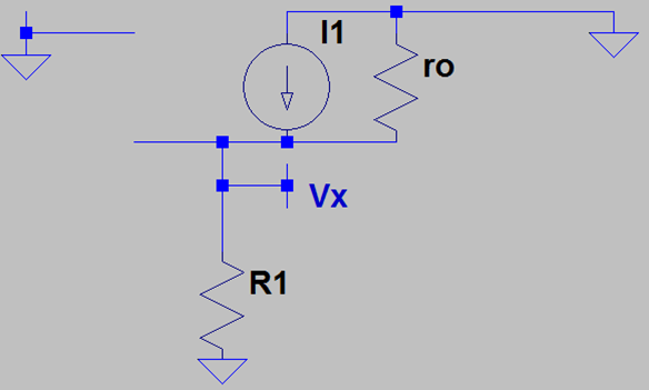
9. In presence of only channel length modulation, what is the output resistance of the following circuit?
a) 1/gm||ro||R2
b) 1/gmb||ro||R2
c) ro||R2
d) 1/(gm-gmb)||ro||R2
View Answer
Explanation: We draw the small signal model of the MOSFET and calculate the resistance looking into the source. Firstly, VGS=-VX and now, we write a KCL at the source i.e. IX+gm*VGS+VX/ro=0. Hence, we find that VX/IX=1/(gm+1/ro) which can be written as 1/gm||ro. Moreover, this resistance is connected to R2 in parallel and we find that the overall resistance is 1/gm||ro||R2.
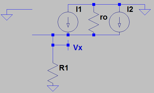
10. In presence of body effect and channel length modulation, what is the output resistance of the following circuit?
a) 1/(gm+gmb)||(ro*R2)
b) 1/(gm+gmb)||(ro-R2)
c) 1/(gm+gmb)||ro||R2
d) 1/(gm+gmb)||(ro+R2)
View Answer
Explanation: We draw the small signal model and observe the ro and RL come in parallel to each other. Moreover, we know that the body effect is expressed as 1/gmb which comes in parallel to 1/gm. The overall output resistance comes out to be
11. What is the voltage gain of the following circuit, if M2 suffers from channel length modulation and M1 suffers from channel length modulation?
a) ro1||ro2/(1/gm+(ro1+ro2))
b) ro1-ro2/(1/gm+(ro1-ro2))
c) ro1||ro2/(1/gm+(ro1||ro2))
d) ro1+ro2/(1/gm+(ro1||ro2))
View Answer
Explanation: The output resistance of M2 is ro2. This resistance is connected to the source of M1 which behaves as a follower since the input is given to the gate and the output is taken from the source. The overall voltage gain becomes ro1||ro2/(1/gm+(ro1||ro2)).
12. What is the voltage gain of the following circuit, if M2 suffers from channel length modulation and M1 suffers from channel length modulation?
a) gm1*(ro1+ro2)/(1+(gm||gmb)(ro1+ro2)
b) gm1*(ro1||ro2)/(1+(gm+gmb)(ro1||ro2)
c) gm1*(ro1||ro2)/(1+(gm+gmb)(ro1+ro2)
d) gm1*(ro1+ro2)/(1+(gm+gmb)(ro1||ro2)
View Answer
Explanation: The output resistance of M2 is ro2. This resistance is connected to the source of M1 which behaves as a follower since the input is given to the gate and the output is taken from the source. The overall voltage gain, in presence of channel length modulation and body effect, becomes gm1*(ro1||ro2)/(1+(gm+gmb)(ro1||ro2).
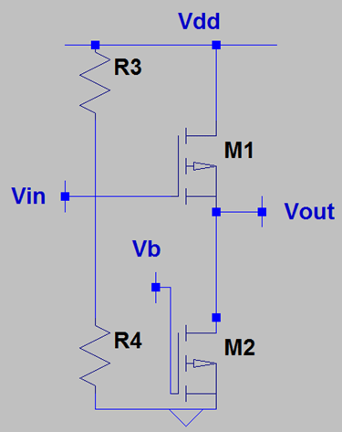
13. State whether the following is true or false.
In the following circuit, body effect will not manifest in M2.
a) True
b) False
View Answer
Explanation: M2 is held at a constant potential. It’s source voltage will always remain equal to the substrate voltage and hence, body effect wont manifest.
14. What is the output resistance of the following circuit, if M1 & M2 suffers from channel length modulation?
a) (1/gm1+ro1)||ro2
b) 1/gm1||(ro1||ro2)
c) 1/gm1||(ro1-ro2)
d) 1/gm1||(ro1+ro2)
View Answer
Explanation: At the output node, we note that that the drain of M2 & the source of M1 are connected. The resistance looking into the drain of M2 is ro2 while the resistance looking into the source of M1 is 1/gm1||ro1. These two resistances appear in parallel to each other and the overall resistance becomes 1/gm1||ro1||ro2.
15. What is the output resistance of the following circuit, if M1 suffers from channel length modulation & body effect while M2 suffers from channel length modulation?
a) (1/gm1+ro1)||ro2
b) 1/(gm+gmb)||(ro1||ro2)
c) 1/gmb||(ro1-ro2)
d) 1/gm1||(ro1+ro2)
View Answer
Explanation: At the output node, we note that that the drain of M2 & the source of M1 are connected. The resistance looking into the drain of M2 is ro2 while the resistance looking into the source of M1 is 1/(gm+gmb)||ro1. These two resistances appear in parallel to each other and the overall resistance becomes 1/(gm+gmb)||(ro1||ro2).
Sanfoundry Global Education & Learning Series – Microelectronics.
To practice all areas of Microelectronics, here is complete set of 1000+ Multiple Choice Questions and Answers.
If you find a mistake in question / option / answer, kindly take a screenshot and email to [email protected]
