This set of Microelectronics Multiple Choice Questions & Answers (MCQs) focuses on “MOS Amplifiers – Common Drain Stage – Set 2”.
1. What is the voltage gain of the following circuit if M1 suffers from Channel length modulation but M2 doesn’t suffer from any second order effect?
a) \(\frac {(r_{o1}+\frac {1}{g_{m2}})}{ (\frac {1}{g_{m}}+(r_{o1}+\frac {1}{g_{m2}}))}\)
b) \(\frac {(r_{o1}+\frac {1}{g_{m2}})}{ (\frac {1}{g_{m}}+(r_{o1}||\frac {1}{g_{m2}}))}\)
c) \(\frac {(r_{o1}||\frac {1}{g_{m2}})}{ (\frac {1}{g_{m}}+(r_{o1}+\frac {1}{g_{m2}}))}\)
d) \(\frac {(r_{o1}||\frac {1}{g_{m2}})}{ (\frac {1}{g_{m}}+(r_{o1}||\frac {1}{g_{m2}}))}\)
View Answer
Explanation: M2 is a PMOS and the MOSFET being a unilateral device, the source will be the terminal which is connected to the higher potential. Hence, the source of M2 is connected to the output node which is connected to the source of M1. The resistance offered by M2 is 1/gm2, at the source end, and the expression of voltage gain becomes \(\frac {(r_{o1}||\frac {1}{g_{m2}})}{ (\frac {1}{g_{m}}+(r_{o1}||\frac {1}{g_{m2}}))}\).
2. What is the voltage gain of the following circuit if M1 & M2 suffers from Channel length modulation?
a) \(\frac {(r_{o1}||\frac {1}{g_{m2}} || r_{o2})}{ (\frac {1}{g_{m}}+(r_{o1}||\frac {1}{g_{m2}} + r_{o2}))}\)
b) \(\frac {(r_{o1}+\frac {1}{g_{m2}} || r_{o2})}{ (\frac {1}{g_{m}}+(r_{o1}||\frac {1}{g_{m2}} || r_{o2}))}\)
c) \(\frac {(r_{o1}||\frac {1}{g_{m2}} || r_{o2})}{ (\frac {1}{g_{m}}+(r_{o1}||\frac {1}{g_{m2}} || r_{o2}))}\)
d) \(\frac {(r_{o1}+\frac {1}{g_{m2}} + r_{o2})}{ (\frac {1}{g_{m}}+(r_{o1}+\frac {1}{g_{m2}} + r_{o2}))}\)
View Answer
Explanation: The source of M2 is connected to the output node which is connected to the source of M1. The resistance offered by M2 is 1/gm2||ro2, due to channel length modulation, at the source end. The expression of voltage gain becomes \(\frac {(r_{o1}||\frac {1}{g_{m2}} || r_{o2})}{ (\frac {1}{g_{m}}+(r_{o1}||\frac {1}{g_{m2}} || r_{o2}))}\). We can always perform a small signal analysis but it becomes a long process. Remembering the expression of voltage gain and representing the MOSFET by a single resistance allows us to simplify the process.
3. What is the voltage gain of the following circuit if M1 & M2 suffers from Channel length modulation and M1 also suffers from Body Effect?
a) gm1*(ro1+1/gm2+ro2)/(1+(gm1||gmb)(ro1+1/gm2+ro2))
b) gm1*(ro1||1/gm2||ro2)/(1+(gm1||gmb)(ro1+1/gm2+ro2))
c) gm1*(ro1+1/gm2+ro2)/(1+(gm1+gmb)(ro1||1/gm2||ro2))
d) gm1*(ro1||1/gm2||ro2)/(1+(gm1||gmb)(ro1||1/gm2||ro2))
View Answer
Explanation: The source of M2 is connected to the output node which is connected to the source of M1. The resistance offered by M2 is 1/gm2||ro2, due to channel length modulation, at the source end. The expression of voltage gain of the follower in presence of channel length modulation and body effect becomes gm1*(ro1||1/gm2||ro2)/(1+(gm||gmb)(ro1||1/gm2||ro2)).
4. What is the voltage gain of the following circuit if M1 & M2 suffers from Channel length modulation and Body Effect?
a) gm1*(ro1||1/(gm2+gmb)||ro2)/(1+(gm1+gmb)(ro1||1/(gm2+gmb)||ro2)
b) gm1*(ro1||1/(gm2+gmb)||ro2)/(1+(gm1+gmb)(ro1||1/(gm2+gmb)||ro2)
c) gm1*(ro1||1/(gm2+gmb)||ro2)/(1+(gm1+gmb)(ro1+1/(gm2+gmb)+ro2)
d) gm1*(ro1||1/(gm2+gmb)||ro2)/(1+(gm1+gmb)(ro1||1/(gm2+gmb)||ro2)
View Answer
Explanation: The source of M2 is connected to the output node which is connected to the source of M1. The resistance offered by M2 is 1/(gm2+gmb)||ro2, due to channel length modulation and body effect, at the source end. The expression of voltage gain of the follower in presence of channel length modulation and body effect becomes gm1*(ro1||1/(gm2+gmb)||ro2)/(1+(gm1+gmb)(ro1||1/(gm2+gmb)||ro2). Note that if M2 will suffer from body effect because the source of the MOSFET is connected to the output node and this leads to a change in the Source voltage with respect to the substrate.
5. What is the output impedance of the following circuit if M1 & M2 doesn’t suffer from any second order effect?
a) 1/gm1
b) 1/gm1||1/gm2
c) 1/gm1+1/gm2
d) Infinite
View Answer
Explanation: The source of M1 & M2 offers an output resistance of 1/gm1 and 1/gm2. Since the output node is connected to the source of each MOSFET, the output resistance becomes 1/gm1||1/gm2.
6. What is the output impedance of the following circuit if M1 & M2 suffer from channel length modulation?
a) (1/gm1+ro1)||(1/gm2+ro1)
b) 1/gm1||ro1-1/gm2||ro1
c) 1/gm1||ro1||1/gm2||ro1
d) 1/gm1||ro1+1/gm2||ro1
View Answer
Explanation: The source of M1 & M2 offers an output resistance of 1/gm1||ro1 and 1/gm2||ro2 respectively. Since the output node is connected to the source of each MOSFET, the output resistance becomes 1/gm1||ro1||1/gm2||ro1.
7. What is the output impedance of the following circuit if M1 & M2 suffer from channel length modulation?
a) 1/(gm1||gmb1)||ro1||1/(gm2||gmb2)||ro2
b) 1/(gm1+gmb2)||ro1||1/(gm2+gmb1)||ro2
c) 1/(gm2+gmb1)||ro1||1/(gm1+gmb2)||ro2
d) 1/(gm1+gmb)||ro1||1/(gm1+gmb)||ro2
View Answer
Explanation: The source of M1 & M2 offers an output resistance of 1/(gm1+gmb)||ro1 and 1/(gm1+gmb)||ro2 respectively. Since the output node is connected to the source of each MOSFET, the output resistance becomes 1/(gm1+gmb)||ro1||1/(gm1+gmb)||ro2.
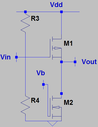
8. What is the behavior of M1 in the following circuit?
a) CG Amplifier
b) Degenerating MOSFET
c) Cascode MOSFET
d) Follower
View Answer
Explanation: M1 behaves as a follower since the input is taken from the gate while the output is taken from the source. It doesn’t take the form of a Cascode since the Cascode stage behaves like a Common Source Stage. Moreover, it doesn’t behave as a degenerating MOSFET since it is not connected to the Source of any MOSFET.
9. What is the behavior of M2 in the following circuit?
a) Amplifier
b) Degenerating MOSFET
c) Cascode MOSFET
d) Follower
View Answer
Explanation: M2 behaves as a degenerating MOSFET since it is connected to the source of M1. It degenerates M1 and hence, the impedance looking into the drain of M1 has increased substantially. Moreover, it behaves as a CS amplifier since the output node is connected to its drain but noting that it is biased at a fixed operating point, the output is considered to be from M1. Note that the impact of VB is present in the output impedance of M2 which does affect the output impedance and in turn the output voltage.
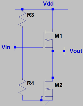
10. What is the voltage gain for the following circuit if channel length modulation is present in both the MOSFETs?
a) \(\frac {(r_{o1}||\frac {1}{g_{m2}}||r_{o2})}{(\frac {1}{g_{m}}+(r_{o1}||\frac {1}{g_{m2}}||r_{o2}))}\)
b) \(\frac {(r_{o1}||\frac {1}{g_{m2}}||r_{o2})}{(\frac {1}{g_{m}}+(r_{o1}+\frac {1}{g_{m2}}+r_{o2}))}\)
c) \(\frac {(r_{o1}||\frac {1}{g_{m2}}+r_{o2})}{(\frac {1}{g_{m}}+(r_{o1}+\frac {1}{g_{m2}}||r_{o2}))}\)
d) \(\frac {(r_{o1}+\frac {1}{g_{m2}}||r_{o2})}{(\frac {1}{g_{m}}+(r_{o1}||\frac {1}{g_{m2}}+r_{o2}))}\)
View Answer
Explanation: M2 behaves as a diode connected device and looking into the source of M2, the impedance is 1/gm2||ro2. The voltage gain is evaluated to be \(\frac {(r_{o1}||\frac {1}{g_{m2}}||r_{o2})}{(\frac {1}{g_{m}}+(r_{o1}||\frac {1}{g_{m2}}||r_{o2}))}\).
Sanfoundry Global Education & Learning Series – Microelectronics.
To practice all areas of Microelectronics, here is complete set of 1000+ Multiple Choice Questions and Answers.
If you find a mistake in question / option / answer, kindly take a screenshot and email to [email protected]
