This set of Microelectronics Multiple Choice Questions & Answers (MCQs) focuses on “MOS Amplifiers – Common Gate Stage”.
1. Neglecting channel length modulation, what is the voltage gain of the following circuit?
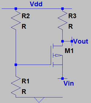
a) gm * R3
b) 2 * gm * R3
c) 0
d) Infinite
View Answer
Explanation: We will have to draw the small signal model of the MOSFET and turn off all independent voltage sources. Next, we apply a voltage at the source and write a simple KCL at the drain end. We observe that ID=-gm * VIN while Vout=-ID*R3. Replacing ID, we have the overall voltage gain as gm * R3.
2. Neglecting channel length modulation, what is the input resistance of the following circuit?
a) 1/gm
b) 2/gm
c) 3/gm
d) Infinite
View Answer
Explanation: We will draw the small signal model of the MOSFET and turn off all independent voltage sources. Now, we apply a voltage at the source and measure the ratio of voltage and current at the source. A KCL does the job as we observe that ID=gm*VS but IS=-ID. Replacing ID, we get the input resistance as 1/gm.
3. Neglecting channel length modulation, what is the output resistance of the following circuit?
a) 2*R3
b) Infinite
c) 0
d) R3
View Answer
Explanation: The output resistance is similar to that of a CS stage. Note that the biasing circuit doesn’t affect the input, output impedances. It also doesn’t hamper the voltage gain as compared to bipolar devices since the current entering through the gate is negligible.
4. In presence of channel length modulation, what is the voltage gain of the following circuit?
a) \(\frac {(1+g_mr_o)}{(3+ r_o/R)}\)
b) \(\frac {(1+g_mr_o)}{(1+ r_o/R)}\)
c) (1+gmro)
d) \(\frac {(1+g_mr_o)}{(1+ 2*r_o/R)}\)
View Answer
Explanation: We draw the small signal model of the MOSFET and turn off all independent sources. Before trying to solve the circuit, we observe that we can convert the combination of current source and the resistor into a voltage source in series with a resistance. Henceforth, the calculation becomes easier as we just need to write a KVL from Vin to Vout. Note that I1=gm*VGS=gm*VIN. The voltage gain becomes \(\frac {(1+g_mr_o)}{(1+ r_o/R)}\).
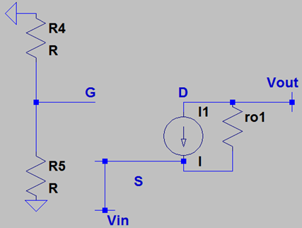
5. In presence of channel length modulation, what is the input impedance of the following circuit?
a) 1/gm + ro
b) 3/gm || ro
c) \(\frac {(R_3+r_O)}{(1+g_m*r_O)}\)
d) 2/gm || ro
View Answer
Explanation: We draw the small signal model and turn of all the independent voltage sources. We apply a voltage at the source end and measure VS/IS. Firstly, we observe that VS(VIN)=-VGS. We write a KCL at the source node and find the current flowing through ro. Next, we write a KVL from R3 to VIN via ro and we have rearrange the terms to get the input impedance as \(\frac {(R_3+r_O)}{(1+g_m*r_O)}\).
6. In presence of channel length modulation, what is the output impedance of the following circuit?
a) ro
b) ro || R3
c) ro || 2*R3
d) ro + R3
View Answer
Explanation: The output impedance is similar to that of a common source stage ie ro || R3. Note that the output impedance doesn’t depend upon whether the input is given to the source and the gate.
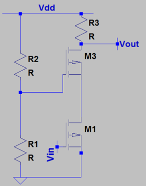
7. In presence of channel length modulation in M2 only , what is the voltage gain?
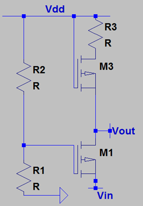
a) gm1*(1/gm3)
b) gm1*(3/gm3*rO3)
c) gm1*(2/gm3*rO3)
d) gm1*(1/gm3*rO3)
View Answer
Explanation: As M1 is behaving as a common gate stage, we observe that the total resistance connected to the drain is (1/gm3*rO3) which is the impedance looking into the source of M3. From the expression of voltage gain of a CG stage, the gain becomes gm1*(1/gm3*rO3).
8. If both the transistors suffer from Channel Length Modulation, what is the voltage gain?
a) (1+gm1)/(5+ro1/(1/gm3*rO3))
b) (1+gm1ro1)/(2+ro1/(1/gm3*rO3))
c) (1+gm1ro1)/(1+ro1/(1/gm3*rO3))
d) (1+ro1)/(4+ro1/(1/gm3*rO3))
View Answer
Explanation: We know that the expression of voltage gain for a C.G. stage is (1+gmro)/(1+ro/1/RD). By replacing RD with (1/gm3*rO3), we get the voltage gain for the following circuit as (1+gm1ro1)/(3+ro1/(1/gm3*rO3)). Note that we can also analyze the cases for when only M2 suffers from Channel Length Modulation and when none of them suffers from Channel Length Modulation. A key point to be remembered is that these resistances only manifest themselves when the voltage is biased, we are calculating these voltage gains in a way that when the these transistors, operating at a certain operating point, suffer from Channel Length Modulation- the voltage gain can be directly obtained from these expressions.
9. If both the transistors suffer from Channel Length Modulation, what is the input impedance?
a) 1/gm || ro
b) 1/gm * ro
c) 1/gm – ro
d) 1/gm + ro
View Answer
Explanation: The input is applied to a MOSFET which is behaving as a CG stage. Hence the input impedance will be similar to that of a CG stage suffering from Channel Length Modulation ie \(\frac {((The \, resistance \, connected \, to \, the \, drain)+r_{O1})}{(1+g_{m1}*r_{O1})}\). The resistance connected to the drain is the resistance looking into the source of M3. This resistance can be calculated by a small signal analysis as \(\frac {(R_3+r_{O3}) } {(1+g_{m3}*r_{O3})}\). The overall resistance becomes \(\frac {((\frac {(R_3+r_{O3})}{1+g_{m3}*r_{O3}})+r_{O1})}{(1+g_{m1}*r_{O1})}\).
10. If only M3 suffers from Channel Length Modulation, what is the input impedance?
a) 2/gm
b) Infinite
c) 1/gm
d) 0
View Answer
Explanation: The input is applied to a MOSFET which is behaving as a CG stage. Hence the input impedance will be similar to that of a CG stage where Channel Length Modulation is neglected ie 1/gm.
11. If only M3 suffers from Channel Length Modulation, what is the output impedance?
a) 2
b) Infinite
c) 1/gm || ro
d) Error in circuit
View Answer
Explanation: To find the output resistance, we observe that the output node is connected to the drain of M1 & the Source of M3. While the former doesn’t offer any output impedance, the output impedance of the latter is 1/gm || ro. The overall output impedance is 1/gm || ro.
12. If both transistors suffer from Channel Length Modulation, what is the output impedance?
a) (1/gm3 || ro3) + ro1
b) Infinite
c) 1/gm3 || ro3 || ro1
d) Error in circuit
View Answer
Explanation: To find the output resistance, we observe that the output node is connected to the drain of M1 & the Source of M3. While the former offers an output impedance of ro1, the output impedance of the latter is 1/gm || ro. The overall output impedance is 1/gm3 || ro3|| ro1.
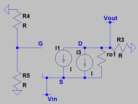
13. In presence of Channel Length Modulation, what is the voltage gain of the following circuit?
a) gm1 * rO1 * gm3 * ro3
b) gm1 * rO1 * gm3 * (R3 + ro)
c) gm1 * rO1 * gm3 * (R3 – ro)
d) gm1 * rO1 * gm3 * (R3 || ro)
View Answer
Explanation: Firstly, we note that the input is applied to M1 and we measure the output from the drain of M3. Hence, the output of M1 travels to the source of M3. We conclude that M1 is part of a CS stage and M3 is behaving in a CG stage. Thereafter, the overall voltage gain is the product of the gain due to both the stages. The first stage offers a gain of gm1 * rO1 while the second stage offers a gain of gm3 * (R3 || ro). The overall gain is gm1 * rO1 * gm3 * (R3 || ro).
14. In presence of Body effect and Channel Length Modulation, what is the voltage gain of the following circuit?
a) \(\frac { \{(g_{mb}+g_m)*r_o + 1 \}R_D}{(r_o + (g_{mb}+g_m)*r_oR_S + R_S + R_D)}\)
b) \(\frac { (g_{mb}+g_m)*r_o + 1 \}R_D}{R_D}\)
c) \(\frac {(g_{mb}+g_m)*r_o + 1 \}R_D}{(r_o + 2R_D)}\)
d) \(\frac { (g_{mb}+g_m)*r_o + 1 \}R_D}{(r_o + R_D)}\)
View Answer
Explanation: Body effect is modelled with a current source from source to drain with the current being gmb*V1 where V1 is the potential difference between the gate (the bulk) and the substrate. Firstly, we conclude that the total current flowing through ro is I1+I2 ie VGS*(gmb+gm). So we replace the two current sources with one current source and convert the combination in to voltage source in series with ro. Now the calculation becomes easier as we write a KVL from VIN to VOUT & the overall voltage gain is \(\frac { (g_{mb}+g_m)*r_o + 1 \} R_D}{(r_o + R_D)}\).
Sanfoundry Global Education & Learning Series – Microelectronics.
To practice all areas of Microelectronics, here is complete set of 1000+ Multiple Choice Questions and Answers.
If you find a mistake in question / option / answer, kindly take a screenshot and email to [email protected]
